Method and apparatus for detecting polysilicon gate etching terminal

A polysilicon gate and detection method technology, applied in the field of microelectronics, can solve the problems of strong sensitivity, inability to reliably protect the gate oxide layer, and difficulty in directly controlling the etching end point, so as to achieve the effect of guaranteed etching

Active Publication Date: 2006-08-02
BEIJING NAURA MICROELECTRONICS EQUIP CO LTD
View PDF1 Cites 10 Cited by
  • Summary
  • Abstract
  • Description
  • Claims
  • Application Information

AI Technical Summary

Problems solved by technology

In this case, the OES endpoint detection method relying only on the plasma emission spectrum cannot reliably protect the gate oxide layer.
[0009] U.S. Patent (U.S 622827) provides a novel endpoint detection method, which uses a bias voltage compensation electrostatic chuck, and performs endpoint detection by monitoring the substrate potential, compensation current or compensation voltage, however, the method Very sensitive, it is difficult to directly control the etching end point
That is to say, relying only on this method is not enough to satisfy polysilicon etching sufficiently and effectively protect the gate oxide of a few nanometers.

Method used


Image

  • Method and apparatus for detecting polysilicon gate etching terminal
  • Method and apparatus for detecting polysilicon gate etching terminal
  • Method and apparatus for detecting polysilicon gate etching terminal

Examples


Embodiment Construction

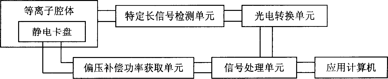
[0042] A detection method and a detection device for a polysilicon gate etching end point according to the present invention, the detection device has specific implementation methods such as figure 2 Shown includes the following units:

[0043] Bias compensation power acquisition unit: used to acquire the bias compensation power information of the electrostatic chuck and output it to the signal processing unit;

[0044] Specific wavelength signal detection unit: used to detect specific wavelength signal information in the polysilicon gate etching cavity, and send it to the photoelectric conversion unit; this embodiment adopts a monochromator;

[0045] Photoelectric conversion unit: convert the specific wavelength signal information into an electrical signal and output it to the signal processing unit; this embodiment uses a photomultiplier tube;

[0046] Signal processing unit: filter and amplify the bias compensation power information and the electrical signal corresponding...


PUM


Abstract

This invention is a kind of end point checking method and checking apparatus of polycrystalline silicon grating etching. The etching process has four steps which have different end point checking method. Bias voltage compensating end point checking predicts the end point of etching process that has relative low etching selecting rate. Use this sensitive method can ensure oxidation layer pre-protected before etching drawing near grate oxygen. Though OES end point checking method, checking etching process of high selecting rate ensures polycrystalline silicon etched fully and grate oxygen layer protected effectively.

Description

technical field [0001] The invention relates to the technical field of microelectronics, in particular to a detection method and a detection device for the etching end point of a polysilicon gate. Background technique [0002] In the manufacture of semiconductor devices, such as the manufacture of integrated circuits or liquid crystal flat panel displays, the raw material for the substrates of these products is generally polysilicon. The polysilicon wafer structure is as follows: [0003] The bottom layer is a silicon wafer; a thin gate silicon oxide of 10-30 angstroms is grown on the silicon wafer; a layer of polysilicon is grown on the gate silicon oxide of 1000-3000 angstroms; a hard mask is grown on the polysilicon; the hard mask can be silicon oxide, nitrogen Silicon oxide, silicon oxynitride; the top of the silicon wafer is the photoresist pattern after photolithography. [0004] The substrate generally needs to be produced in a plasma chamber environment, and photol...

Claims


Application Information

Patent Timeline
Patent Type & Authority Applications(China)
IPC IPC(8): H01L21/66
Inventor 许仕龙
Owner BEIJING NAURA MICROELECTRONICS EQUIP CO LTD
Why Eureka
Try Eureka