Process for preparing low-temperature wafer-level mini-sized gas container

A wafer-level, gas-based technology, applied in nanostructure manufacturing, nanotechnology, nanotechnology, etc., can solve problems such as the difficulty of making chip-level atomic clocks, achieve reduced residual thermal stress, low processing costs, and prevent element loss Effect

Inactive Publication Date: 2006-09-06
SHANGHAI INST OF MICROSYSTEM & INFORMATION TECH CHINESE ACAD OF SCI
View PDF0 Cites 11 Cited by
  • Summary
  • Abstract
  • Description
  • Claims
  • Application Information

AI Technical Summary

Problems solved by technology

The gas bubbles made by this method are usually on the order of centimeters in diameter, so it is difficult to make a highly integrated system-level chip-scale atomic clock on this basis.

Method used


Image

  • Process for preparing low-temperature wafer-level mini-sized gas container
  • Process for preparing low-temperature wafer-level mini-sized gas container
  • Process for preparing low-temperature wafer-level mini-sized gas container

Examples


Embodiment 1

[0097] The chip-level atomic clock gas box is fabricated by wet etching silicon material, and the specific process is as follows Figure 4 , as shown in 5. The process steps are as follows:

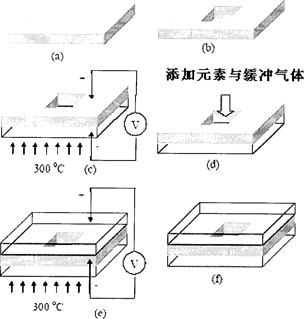
[0098] (1) Select a semiconductor material such as silicon wafer 1 (ordinary N-type (100) double-polished silicon wafer, thickness 420±15 μm, resistivity 3-8 (Ω cm)), and oxidize to obtain the top mask silicon dioxide 2 and underlying silica 3, such as Figure 4 (b);

[0099] (2) Coat photoresist 4 (in this experiment, adopt the trade mark 1912 photoresist of Shipley Company), after curing, protect the top mask silicon dioxide 2, remove the bottom layer silicon dioxide 3 in BOE etching solution, as Figure 4 (d);

[0100] (3) After removing the cured photoresist, apply photoresist 4 again and pattern exposure and development to obtain the following: Figure 4 (e) structure;

[0101] (4) corrode top layer mask silicon dioxide 2 in BOE etching solution, open etching window for it, rem...

Embodiment 2

[0110] The chip-level atomic clock gas box is made by dry etching silicon material, and the specific process is as follows Figure 4 , as shown in 5. The process steps are as follows:

[0111] (1) Select a semiconductor material such as silicon wafer 1 (ordinary N-type (100) double-polished silicon wafer, thickness 420±15 μm, resistivity 3-8 (Ω cm)), apply photoresist 4 and pattern exposure, developed, obtained as Figure 4 (k) structure;

[0112] (2) Under the patterned mask of photoresist, the Figure 4 (k) The structure is etched by dry reactive particle to obtain as Figure 4 (1) structure;

[0113] (3) Carry out anodic bonding of silicon wafer 1 and Pyrex7740 glass 5 under normal standard process (temperature 380°C, voltage ±800V), such as Figure 4 (m) cavity structure;

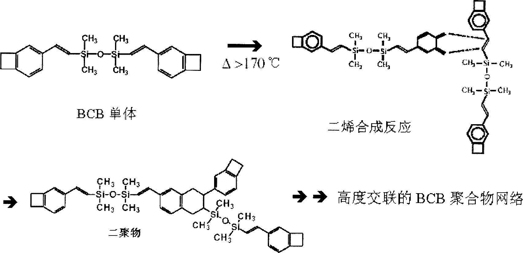
[0114] (4) In Pyrex (Pyrex) 7740 glass 5 or as Figure 4 (m) spin-coating or spraying BCB glue 6 on the top surface of the cavity structure, the concrete coating process parameters are with refe...

Embodiment 3

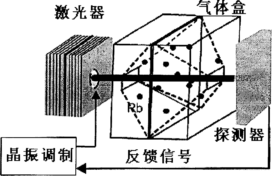
[0119] The high-precision magnetic field sensor gas box is made of wet-etched silicon material. The structure of the high-precision magnetic field sensor based on atomic energy level transition is as follows: Figure 12 As shown, it includes a semiconductor vertical cavity emitting laser 9 , an optical adjustment and collimation system 10 , an Rb element vapor cavity 11 , and a photodetector 12 . The manufacturing process steps of its core component—the Rb element steam chamber 11 are as follows:

[0120] (1) Select a semiconductor material such as a silicon wafer 1 (ordinary N-type (100) double-polished silicon wafer, thickness 420±15 μm, resistivity 3-8 (Ω cm)), and oxidize to obtain the top layer mask silicon dioxide 2 and underlying silica 3, such as Figure 4 (b);

[0121] (2) Coat photoresist 4 (in this experiment, adopt the trade mark 1912 photoresist of Shipley Company), after curing, protect the top mask silicon dioxide 2, remove the bottom layer silicon dioxide 3 i...


PUM


Abstract

The invention relates to a method for producing low-temperature circle sheet micro gas box, which is characterized in that: the benzocyclobutene is used to process material linkage with humid etching or dry etching technique of semi-conductor in 250Deg. C, to realize the circle sheet air-tightness sealing linkage of chip-level gas box. The invention comprises a atom gas box containing a chip-level atom clock gas box, a high-precision magnetic field sensor gas box, a atom feedback glimmer frequency stabilizer; a atom gas box containing a atom light filter, with glimmer Fabry-Perot chamber. The linked BCB glue is in 0.2ª–m thickness, the air-tightness of sealed He gas can reach 2.1-5.9X10⁻⁴Pa cm3/s, and the linkage strength is higher than 4.65MPa, while the thermal cycle reliability can fully reach the packing standard of micro electric device.

Description

technical field [0001] The invention relates to a manufacturing method of a low-temperature wafer-level miniature gas box, in particular, a method for using benzocyclobutene (BCB) material to conduct low-temperature processing of semiconductor materials or glass that have been wet-etched or dry-etched. Wafer-level hermetic bonding enables the fabrication of chip-level gas boxes. The invention belongs to the technical field of micro-photoelectric devices and micro-processing. Background technique [0002] Some MEMS devices, such as chip-level atomic clocks, microatomic magnetic field sensors, gas boxes for laser frequency stabilization devices, and atomic filters, require strict airtight packaging due to their physical working principles, stable operation, and low drift requirements. With the development of semiconductor technology towards systematization and integration, lower requirements are placed on the bonding temperature in the device manufacturing process. Wafer-lev...

Claims


Application Information

Patent Timeline
Patent Type & Authority Applications(China)
IPC IPC(8): B82B3/00
Inventor 刘玉菲吴亚明李四华刘文平
Owner SHANGHAI INST OF MICROSYSTEM & INFORMATION TECH CHINESE ACAD OF SCI
Why Eureka
Try Eureka