Thin film semiconductor and method for manufacturing the same, semiconductor device and method for manufacturing the same

A technology of thin-film transistors and semiconductors, applied in semiconductor/solid-state device manufacturing, transistors, electrical components, etc., can solve problems such as uncontrollable positions, and achieve an effect that is conducive to industrial production

Inactive Publication Date: 2007-02-07
SEMICON ENERGY LAB CO LTD
View PDF0 Cites 0 Cited by
  • Summary
  • Abstract
  • Description
  • Claims
  • Application Information

AI Technical Summary

Problems solved by technology

According to the conventional technique, a point (for example, the concave-convex portion 302 shown in Fig. 3(A) ) which will become the freezing point of the component is formed regularly, and its position cannot be controlled

Method used


Image

  • Thin film semiconductor and method for manufacturing the same, semiconductor device and method for manufacturing the same
  • Thin film semiconductor and method for manufacturing the same, semiconductor device and method for manufacturing the same
  • Thin film semiconductor and method for manufacturing the same, semiconductor device and method for manufacturing the same

Examples


Embodiment 1

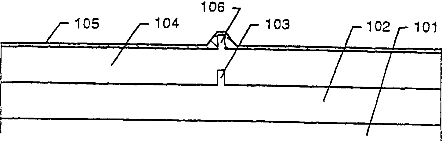
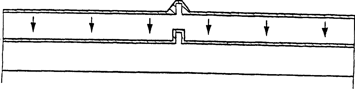
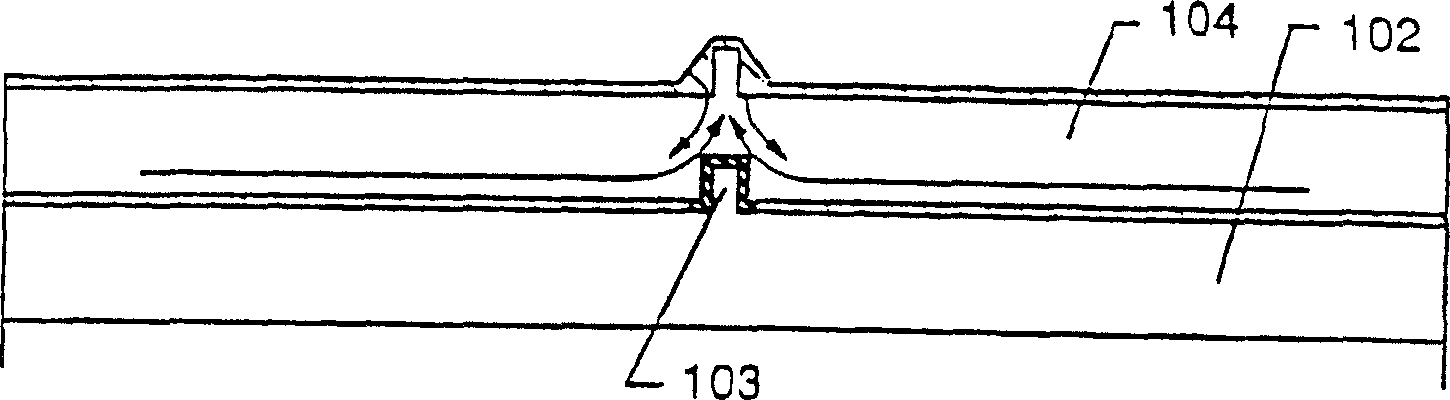
[0073] This embodiment describes the formation process of the monodomain region, which is the most important idea of ​​the present invention. Figure 1(A)-1(F) is a cross-sectional view of silicon formed on a substrate with an insulating surface.

[0074] Referring to FIG. 1(A), a silicon oxide film 102 is formed on a glass substrate 101 by sputtering. A quartz substrate or a silicon substrate may also be used instead of the glass substrate. Artificial quartz targets are used in sputtering. The surface of the silicon oxide film 102 formed using the artificial quartz target is extremely flat and smooth. More specifically, for example, the surface roughness has a height in the range of 30 Ȧ and a width of 100 Ȧ or more. Even with AFM (atomic force microscope) observation, it is difficult to find irregularities.

[0075] After the silicon oxide film 102 is formed, patterning is performed to form the uneven pattern 103 intentionally. In this embodiment, a micro-island-like sq...

Embodiment 2

[0124] This embodiment is similar to that described in Embodiment 1, except that the laser irradiation is replaced by strong light with the same energy as the laser. The known RTA (Rapid Thermal Annealing) technique is used in this embodiment.

[0125] RTA is a method of irradiating a workpiece with strong light such as infrared light or ultraviolet light generated by a lamp or the like. This method is characterized in that it can complete the treatment in a short time of about several to tens of seconds, and can heat and cool at a high speed. In this way, only the film on the outermost surface can be heated. More specifically, for example, only a thin film on the surface of a glass substrate can be annealed at an extremely high temperature of about 1000°C.

[0126] Using this method, the processing time is short, and the output can be greatly improved during production. Therefore, this method is very effective for improving productivity.

Embodiment 3

[0128] This embodiment is an example of an active layer of a thin film transistor formed using the monodomain region obtained in the process steps described in Embodiment 1. Although a top-gate structure is described in this embodiment, it can also be used in a bottom-gate structure.

[0129] Referring to FIG. 4(A), according to the process steps described in Embodiment 1, a thin film transistor including a single domain region is formed and patterned. An active layer 403 consisting of only monodomain regions is formed. Also, as described in Embodiment 1, reference numeral 401 denotes a glass substrate, and reference numeral 402 denotes a silicon oxide film.

[0130] Then, a silicon oxide film 404 serving as a gate insulating film was formed to a thickness of 1500 Ȧ by plasma CVD. A silicon oxynitride film or a silicon nitride film may also be used instead of the silicon oxide film.

[0131] Thereafter, an aluminum film 405 was formed to a thickness of 5000 Ȧ by sputtering ...


PUM


Abstract

The present invention is related to a thin film semiconductor which can be regarded as substantially a single crystal and a semiconductor device comprising an active layer formed by the thin film semiconductor. At least a concave or convex pattern is formed intentionally on a insulating film provided in contact with the lower surface of an amorphous silicon film, whereby at least a site is formed in which a metal element for accelerating crystallization can be segregated. Therefore, a crystal nuclei is selectively formed in a portion where the concave or convex pattern is located, which carries out controlling a crystal diameter. Thus, a crystalline silicon film is obtained. A crystallinity of the crystalline silicon film is improved by the irradiation of a laser light or an intense light having an energy equivalent to that of the laser light, whereby a monodomain region in which no grain boundary substantially exit is formed.

Description

[0001] This application is an invention patent application with an application date of February 23, 1997, a divisional submission date of April 14, 2004, an application number of 200410034293.1, and an invention title of "thin-film semiconductor, semiconductor device, and method for manufacturing a thin-film transistor" divisional application. technical field [0002] The invention relates to a thin film semiconductor, and also relates to a semiconductor device using the thin film semiconductor as an active layer. In particular, it relates to a thin film transistor whose active layer is formed of a crystalline silicon film. Background technique [0003] In recent years, a technique of forming a thin film transistor from a thin silicon film (thickness of several hundred to several thousand Å) formed on a substrate having an insulating surface has attracted great attention. Thin film transistors have been widely used in electronic devices such as ICs and liquid crystal displa...

Claims


Application Information

Patent Timeline
Patent Type & Authority Applications(China)
IPC IPC(8): H01L21/336H01L29/786
Inventor 山崎舜平宫永昭治小山润福永健司
Owner SEMICON ENERGY LAB CO LTD
Why Eureka
Try Eureka