Simple-beam type microelectronic mechanical system detection card and producing method thereof

A micro-electromechanical, beam-type technology, applied in the field of integrated circuit testing, can solve problems such as unbearable, and achieve the effects of expanding adaptability, high engraving accuracy, and cost saving

Inactive Publication Date: 2007-03-28
SHANGHAI JIAO TONG UNIV
View PDF0 Cites 13 Cited by
  • Summary
  • Abstract
  • Description
  • Claims
  • Application Information

AI Technical Summary

Problems solved by technology

The main problem with this type of MEMS probe is that as the size of the probe continues to decrease, it cannot withstand and generate the stress required to destroy the natural oxide layer or contamination layer on the surface of the metal pin.

Method used


Image

  • Simple-beam type microelectronic mechanical system detection card and producing method thereof
  • Simple-beam type microelectronic mechanical system detection card and producing method thereof
  • Simple-beam type microelectronic mechanical system detection card and producing method thereof

Examples


Embodiment 1

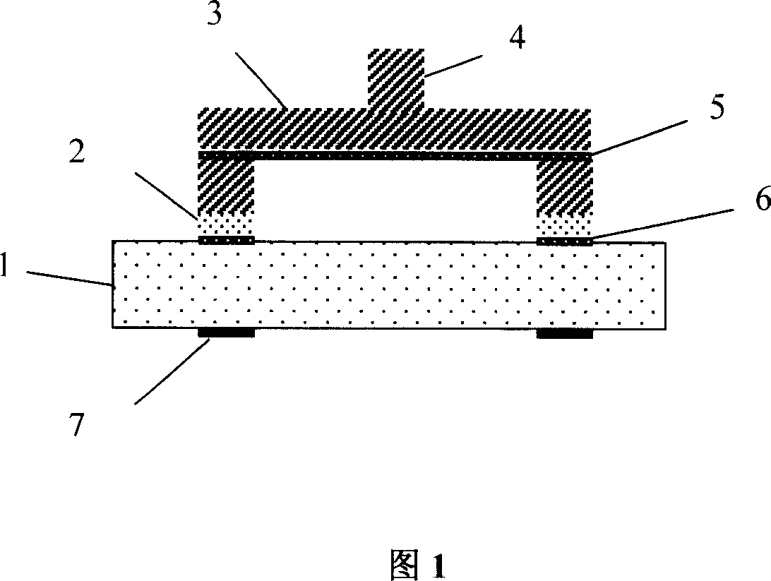
[0030] Simple supported beam structure parameters: beam thickness 15μm, probe diameter 30μm, probe height 25μm.

[0031] (1) Alignment symbol production on the back

[0032] Using a glass sheet with a thickness of 2 mm as the substrate, the substrate is first processed: ultrasonically cleaned with acetone, alcohol and deionized water, and dried in a vacuum oven at 180°C for 3 hours. Then on the back of the substrate, 100nm thick chromium is sputtered, 2μm thick AZ4620 is coated on the top of the chromium. After photolithography and development, the chromium is etched with 8% hydrochloric acid, and the photoresist is removed with acetone to obtain the chromium. Align the symbol mark on the back.

[0033] (2) Metal lead production

[0034] Wipe the front surface of the substrate without metal alignment symbols with acetone, ultrasonically clean with deionized water, and place it in a vacuum oven for drying. Sputter a 100nm bottom Cr / Cu seed layer, apply 7μm thick positive glue AZ462...

Embodiment 2

[0040] Simple supported beam structure parameters: beam thickness 10μm, probe tip diameter 30μm, probe tip height 25μm.

[0041] (1) Alignment symbol production on the back

[0042] Using a glass sheet with a thickness of 2mm as the substrate, the substrate is first processed: ultrasonically cleaned with acetone, alcohol and deionized water, and dried in a vacuum oven at 180°C for 3 hours. Then on the back of the substrate, 100nm thick chromium is sputtered, 2μm thick AZ4620 is coated on the top of the chromium. After photolithography and development, the chromium is etched with 8% hydrochloric acid, and the photoresist is removed with acetone to obtain the chromium. Align the symbol mark on the back.

[0043] (2) Metal lead production

[0044] Wipe the front surface of the substrate without metal alignment symbols with acetone, ultrasonically clean with deionized water, and place it in a vacuum oven for drying. Sputtering a 100nm bottom Cr / Cu seed layer, coating 7μm thick positiv...

Embodiment 3

[0050] Simple supported beam structure parameters: beam thickness 15μm, probe tip diameter 10μm, probe tip height 50μm.

[0051] (1) Alignment symbol production on the back

[0052] Using a glass sheet with a thickness of 2mm as the substrate, the substrate is first processed: ultrasonically cleaned with acetone, alcohol and deionized water, and dried in a vacuum oven at 180°C for 3 hours. Then on the back of the substrate, 100nm thick chromium is sputtered, 2μm thick AZ4620 is coated on the top of the chromium. After photolithography and development, the chromium is etched with 8% hydrochloric acid, and the photoresist is removed with acetone to obtain the chromium. Align the symbol mark on the back.

[0053] (2) Metal lead production

[0054] Wipe the front surface of the substrate without metal alignment symbols with acetone, ultrasonically clean with deionized water, and place it in a vacuum oven for drying. Sputter a 100nm bottom Cr / Cu seed layer, apply 7μm thick positive glu...


PUM


Abstract

This invention relates to a simple beam MEMS explore cards preparation methods, using UV-LIGA many lithography, preparation of flexible probe in the metal films with electroplating process, using the simple structure probe instead of the cantilever beam to bear the stress and greater oxide film holes, and regulate the probe displacement through the design of thickness of simple beams. Chip cards in accordance with the present invention, are obtained by the joint distribution and arrangement of the functions of the simple beam array, simply supported beam probe in the middle, and ensure the location of the needle position consistent with the corresponding pin chip. The bottom end of SR beam is the plating metal wire, which external from the bottom end around to the probe extension spot welding to connect to the corresponding printed circuit board, thus testing machine connected to the signal from the probe circuit. The invention process is simple, high productivity, control probe shape and size very well, high accuracy, suitable for mass production.

Description

Technical field [0001] The invention relates to a microelectronic mechanical system probe card and a preparation method thereof, in particular to a simple beam type microelectronic mechanical system probe card for chip testing and a preparation method thereof, and belongs to the technical field of integrated circuit testing. Background technique [0002] Semiconductor wafer testing is to check the ideal work of the wafer and the integrated circuit on the wafer by performing electrical tests including short circuit, open circuit, AD / CD and function on the wafer and the integrated circuit on the wafer in the uncut state. Status, so as to find ways to increase yield, reduce chip manufacturing costs and improve chip functions. With the development of VLSI (Very Large Scale Integrated Circuit) technology toward greater integration and higher speed, the number of I / Os has increased sharply, and the size and spacing of chip pins have been reduced accordingly. In this way, not only the m...

Claims


Application Information

Patent Timeline
Patent Type & Authority Applications(China)
IPC IPC(8): G01R1/02G01R1/067G01R1/073G01R31/00G01R31/02G01R31/28G01R31/26H01L21/66
Inventor 靖向萌陈迪张晔黄闯陈翔刘景全
Owner SHANGHAI JIAO TONG UNIV
Why Eureka
Try Eureka