Scatheless grinding method for rigid, fragile crystal wafer

A substrate and crystal technology, applied in the field of ultra-precision processing of hard and brittle crystal substrates, can solve the problems of environmental pollution, low processing efficiency, high processing cost, etc., and achieve high material removal rate, high grinding precision, and low processing cost Effect

Active Publication Date: 2007-05-09
DALIAN UNIV OF TECH
View PDF0 Cites 17 Cited by
  • Summary
  • Abstract
  • Description
  • Claims
  • Application Information

AI Technical Summary

Problems solved by technology

However, in the chemical mechanical polishing process, there are disadvantages such as difficult control of the substrate surface shape, high processing cost, low processing efficiency, difficult cleaning of the crystal substrate, and enviro

Method used


Image

  • Scatheless grinding method for rigid, fragile crystal wafer
  • Scatheless grinding method for rigid, fragile crystal wafer
  • Scatheless grinding method for rigid, fragile crystal wafer

Examples


Embodiment Construction

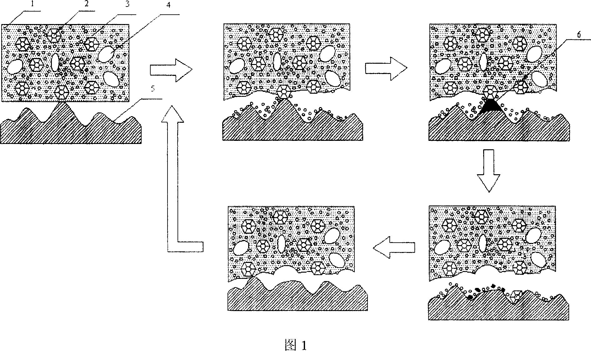
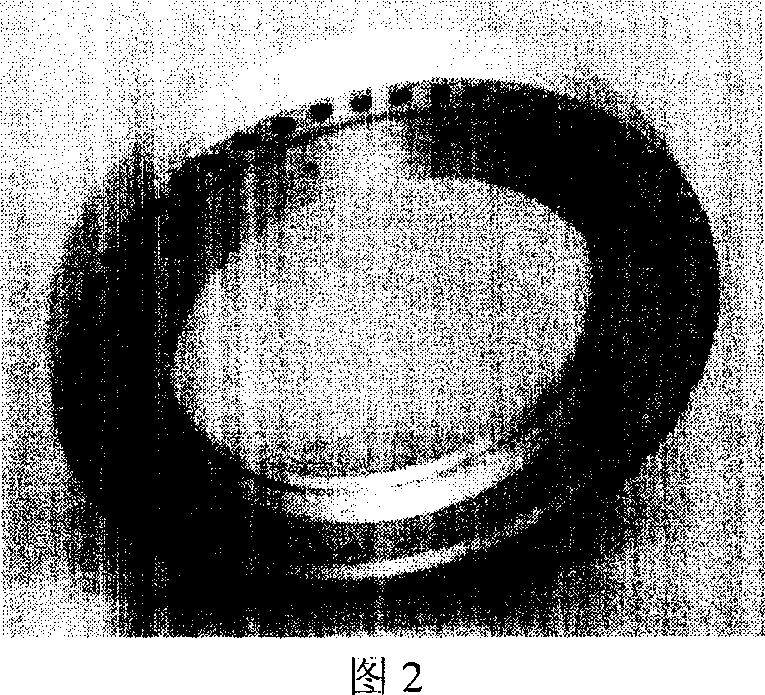
[0012] The specific implementation of the present invention will be described in detail in conjunction with the accompanying drawings. Using VG401 MKII ultra-precision wafer grinder, using a single crystal silicon substrate as a sample, using #3000 ceria abrasive (harder than single crystal silicon substrate), resin adhesive and surfactant, strong acid and weak alkali salt The grinding wheel made of fillers such as pH regulator, oxidizing agent, etc., the actual grinding wheel is shown in Figure 2. Install the grinding wheel on the spindle of the VG401MKII ultra-precision grinding machine. The dressing disc adopts a diamond grinding wheel electroplated on the metal substrate. Next, the monocrystalline silicon substrate is fixed on the grinding machine on the clamping table; the grinding feed rate is selected as 1 μm / min, the rotation speed of the grinding wheel is 600 n / min, and the rotation speed of the hard and brittle crystal substrate is 80 n / min. Ionized water is used as...


PUM


Abstract

A nondestructive grinding method for the hard and crisp crystal substrate of semiconductor or photoelectric crystal features used of a special abrasive disc prepared from the grinding material chosen from CeO2, SiO2 and barium carbonate and the filler containing activator, oxidant and pH regulator, a finishing disc composed of metallic substrate and electroplated diamond particles, and a deionized water as cooling liquid. Its grinding parameters are also disclosed.

Description

technical field [0001] The invention belongs to the technical field of ultra-precision processing of hard and brittle crystal substrates, in particular to the ultra-precision grinding processing technology of hard and brittle crystal substrates of semiconductors and photoelectric crystals. Background technique [0002] With the rapid development of semiconductor and optoelectronic technology, the processing accuracy and surface quality requirements of the basic substrate material - hard and brittle crystal substrate are becoming more and more stringent. On the one hand, the processed surface of the wafer is required to have sub-micron geometric precision; on the other hand, it is also required to have a high surface / sub-surface integrity, and the surface roughness of the wafer is required to reach the sub-nanometer level, and there are no micro-cracks, micro-scratches, Defects such as micro-defects, and the sub-surface layer is required to be free from processing damage such...

Claims


Application Information

Patent Timeline
IPC IPC(8): B24B7/22B24D3/00B24B53/04H01L21/304
Inventor 郭东明田业冰康仁科金洙吉高航
Owner DALIAN UNIV OF TECH
Why Eureka
Try Eureka