Micro mechanical capacitance type acceleration transducer, and fabricating method
A technology of an acceleration sensor and a manufacturing method, which is applied in the direction of measuring acceleration, velocity/acceleration/impact measurement, instruments, etc., can solve the problems of increasing the difficulty and complexity of manufacturing process, increasing the complexity of manufacturing process, difficulty in controlling the size and shape, and the like, The layout design is simple, the manufacturing cost is reduced, and the sensitivity is changed.
- Summary
- Abstract
- Description
- Claims
- Application Information
AI Technical Summary
Problems solved by technology
Method used
Image
Examples
Embodiment 1
[0048] 1. Corrosion forms the damping gap window of the movable mass block, that is, the production of the intermediate movable mass block:
[0049] (1) The upper and lower surfaces of the oxidized double-polished (100) silicon wafer are made of damping gap window 5 by anisotropic etching method, and the etching depth is 4um;
[0050] (2) Secondary oxidation to form silicon oxide, double-sided photolithography, using chemical vapor deposition process to fabricate 4000 Ȧ Si on the upper and lower surfaces of the movable mass 3 N 4 Anti-overload bump 7;
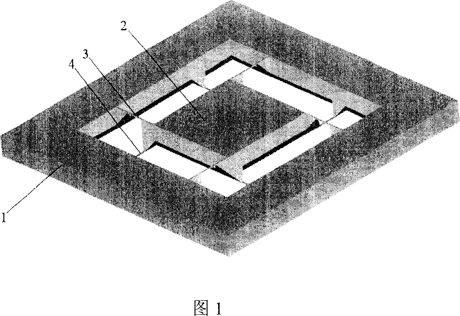
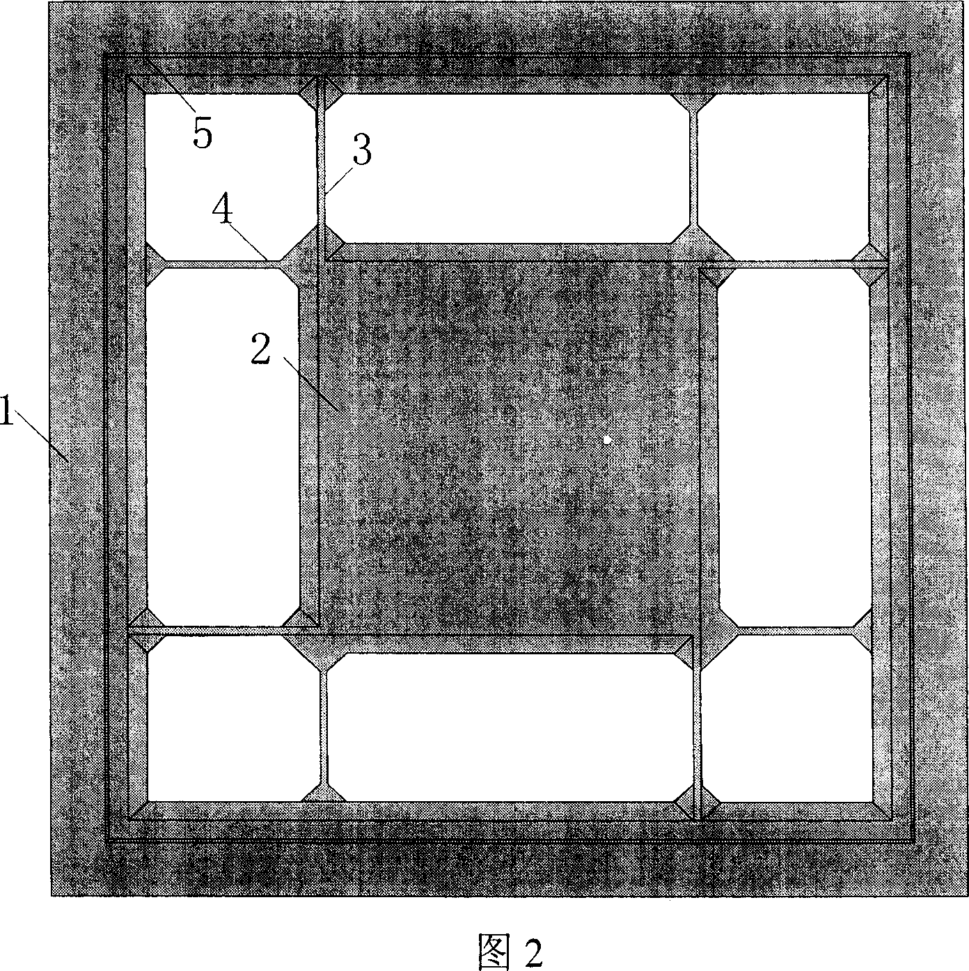
[0051] (3) Upper and lower double-sided photolithographic patterns, wet anisotropic etching to obtain straight elastic beams 3, 4 and movable mass 2 on the front and back of the movable electrode at the same time, the etching depth is determined by the thickness of the silicon wafer and the elastic beam depends on the thickness. There are four straight elastic beams 3 on the front side of the silicon wafer, which are distrib...
Embodiment 2
[0059] Its concrete implementation steps are identical with embodiment 1, and main difference is the distribution (Fig. 6) of straight elastic beam:
[0060] There are four straight elastic beams 3 on the front side of the silicon wafer 1 distributed symmetrically on the opposite corners of the mass block;
[0061] Four straight elastic beams 4 are symmetrically distributed on the corners of the other two opposite sides of the mass block on the back of the silicon wafer 1 .
Embodiment 3
[0063] 1. Production of the middle movable mass:
[0064] (1) The upper and lower surfaces of the oxidized double-polished (100) silicon wafer are made of damping gap window 5 by anisotropic etching method, and the etching depth is 4um;
[0065] (2) Secondary oxidation to form silicon oxide, double-sided photolithography, using chemical vapor deposition process to produce 4000 Ȧ Si on the upper and lower surfaces of the mass block 3 N 4 Anti-overload bump 7.
[0066] (3) Front photolithographic pattern, wet anisotropic etching to obtain straight elastic beam 3 and movable mass block 2 at the same time;
[0067] (4) Secondary oxidation, photolithographic pattern on the back, and wet anisotropic etching to obtain the straight elastic beam 4 and the movable mass block 2 at the same time. The depth of the two etchings is the same, which is determined by the thickness of the silicon wafer and the thickness of the elastic beam. . There are four straight elastic beams 3 on the fr...
PUM
 Abstract
Description
Claims
Application Information


