Ring-shaped magnetic multi-layer film and method for making same and use

A multi-layer film and magnetic technology, applied in the application of magnetic film to substrate, magnetic layer, multi-layer film with spin exchange coupling, etc., can solve the problem of complex structure design and preparation of memory cells, increasing free layer inversion issues such as field and power consumption

Active Publication Date: 2007-07-04
INST OF PHYSICS - CHINESE ACAD OF SCI
View PDF0 Cites 19 Cited by
  • Summary
  • Abstract
  • Description
  • Claims
  • Application Information

AI Technical Summary

Problems solved by technology

However, due to the geometric structure of memory cells (such as bit layers and other pinning layers) used in the prior art adopts non-closed structures, such as rectangles, ellipses, etc., this structure will lead to high density and small size memory cells. Larger demagnetization field and shape anisotropy, this defect will undoubtedly increase the reversal field and power cons

Method used


Image

  • Ring-shaped magnetic multi-layer film and method for making same and use
  • Ring-shaped magnetic multi-layer film and method for making same and use

Examples


Embodiment 1

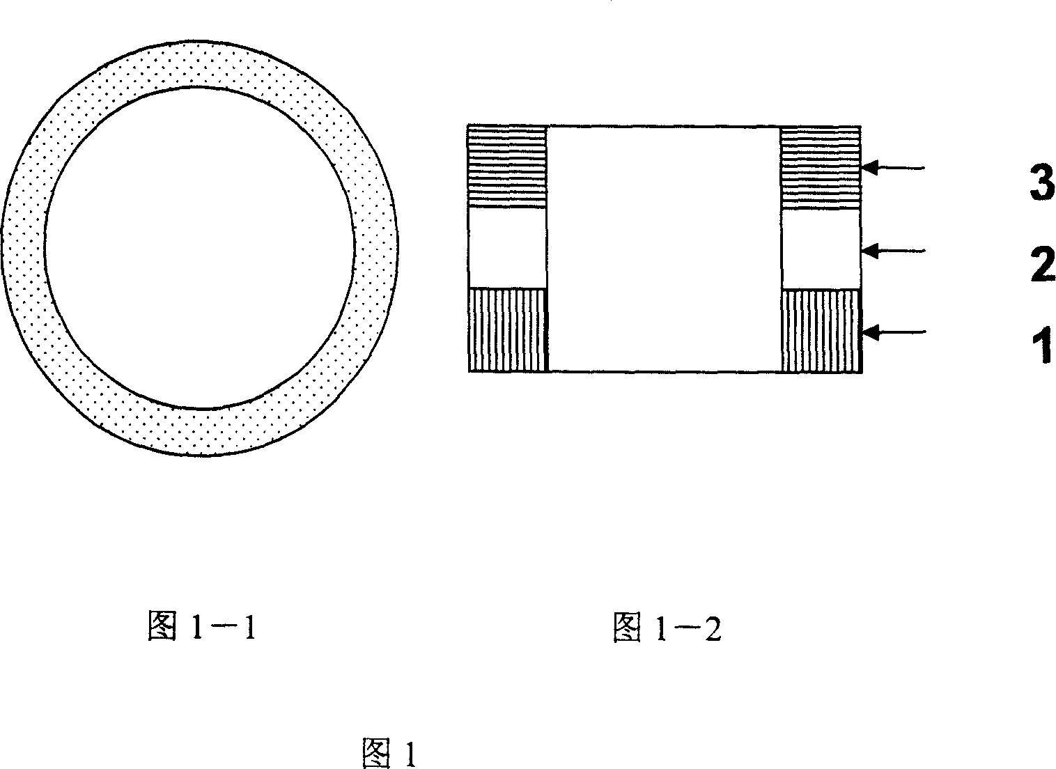
[0053] Example 1. Preparation of non-pinning annular magnetic multilayer film by micromachining method

[0054] Using high-vacuum magnetron sputtering equipment in the 1mm thick SiO cleaned by conventional methods 2 On the Si substrate, the lower buffer conductive layer Au with a thickness of 2nm, the hard magnetic layer (HFM) Co with a thickness of 3nm, the intermediate layer (I1) Cu with a thickness of 1nm, and the soft magnetic layer (SFM) with a thickness of 1nm were deposited sequentially. Co and a cap layer Ru with a thickness of 4 nm. The growth conditions of the above-mentioned magnetic multilayer film: prepared vacuum: 5×10 -7 Pa; high-purity argon gas pressure for sputtering: 0.07 Pa; sputtering power: 120 watts; sample holder rotation rate: 20rmp; growth temperature: room temperature; Rate; when depositing hard magnetic layer and soft magnetic layer, apply a 50Oe plane induced magnetic field. The deposited magnetic multilayer film adopts the micro-processing tech...

Embodiment 2

[0055] Example 2. Preparation of non-pinning annular magnetic multilayer film by using insulator nanoparticle mask method

[0056] Using high-vacuum magnetron sputtering equipment on 0.3mm thick Si / SiO cleaned by conventional methods 2 A lower buffer conductive layer of Au with a thickness of 2nm is sequentially deposited on the substrate, and a layer of SiO with a diameter of 100nm is dispersed on the lower buffer conductive layer. 2 particles, and then use high-vacuum magnetron sputtering equipment to sequentially grow a hard magnetic layer (HFM) Co with a thickness of 20nm 75 Fe 25 , an intermediate layer (I1)Cr with a thickness of 10nm, a soft magnetic layer (SFM)Co with a thickness of 10nm 75 Fe 25 and a capping layer Ta with a thickness of 10 nm. The growth conditions of the above-mentioned magnetic multilayer film: prepared vacuum: 5×10 -7 Pa; high-purity argon gas pressure for sputtering: 0.07 Pa; sputtering power: 120 watts; sample holder rotation rate: 20rmp; gr...

Embodiment 3

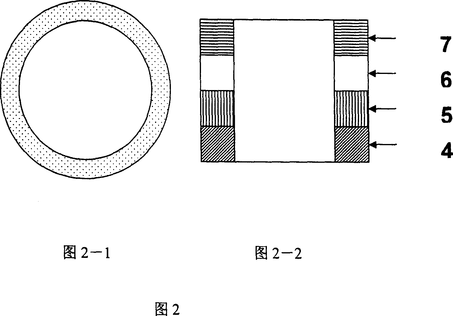
[0057] Example 3. Preparation of pinned annular magnetic multilayer film by micromachining method

[0058] Using high vacuum magnetron sputtering equipment to clean 0.8mm thick Si / SiO by conventional methods 2 The lower buffer conductive layer Au with a thickness of 2 nm, the antiferromagnetic pinning layer (AFM) IrMn with a thickness of 10 nm, and the pinned magnetic layer (FM1) Co with a thickness of 3 nm were sequentially deposited on the substrate. 90 Fe 10 ; then deposit 1nm of Al, the insulating layer formed through plasma oxidation for 50 seconds as the intermediate layer (I2); on this intermediate layer, the free soft magnetic layer (FM2) Co with a thickness of 3nm is deposited successively 90 Fe 10 and a capping layer of Au with a thickness of 2 nm. The growth conditions of the above-mentioned magnetic multilayer film: prepared vacuum: 5×10 -7 Pa; high-purity argon gas pressure for sputtering: 0.07 Pa; sputtering power: 120 watts; sample holder rotation rate: 20rm...


PUM

PropertyMeasurementUnit
The inside diameter ofaaaaaaaaaa
Outer diameteraaaaaaaaaa
Thicknessaaaaaaaaaa

Abstract

This invention relates to a circular magnetic multi-layer membrane, which characterized with: the cross section of the said magnetic multi-layer membrane takes on the closed circle shape, the circle's inner diameter being 10~100000nm, outer diameter being 20~200000nm. In accordance with the classification of the forming materials, the magnetic multi-layer membrane of the invention includes the circular magnetic multi-layer membrane without pinning and the circular magnetic multi-layer membrane with pinning, and it can be prepared through micro-processing method or insulator micron, submicron or nano-particles masking method. The circular magnetic multi-layer membrane of the invention has no fading magnetic field, weak shape anisotropy, and it can be widely used in various devices with the core of magnetic multi-layer membrane, such as magnetic random access memory, computer magnetic heads, magnetic-sensing sensors, etc.

Description

technical field [0001] The invention relates to an annular magnetic multilayer film, its preparation method, and its application in devices. Background technique [0002] Since Baibich et al first observed the giant magnetoresistance (Giant Magneto Resistance, GMR) effect in the magnetic multilayer film system in the late 1980s, the research on the magnetic multilayer film system has been a topic of general concern to researchers. Because the GMR effect has a high magnetoresistance ratio, it can be widely used in magnetoresistance sensors, magnetic recording and reading heads, and other fields. Devices made of GMR not only have excellent characteristics such as high sensitivity, small size, and low power consumption, but can also bring many new features such as radiation resistance and non-volatile information storage. In particular, the application of the GMR effect to magnetic recording and reading heads has brought a profound revolution to the entire field of information...

Claims


Application Information

Patent Timeline
IPC IPC(8): H01F10/32H01F10/12H01F41/14H01L43/08H01L43/12G11C11/16G11B5/39
Inventor 马明韩秀峰姜丽仙韩宇男覃启航魏红祥
Owner INST OF PHYSICS - CHINESE ACAD OF SCI
Why Eureka
Try Eureka