X-ray scatterometry metrology for high aspect ratio structures

a high aspect ratio, x-ray scatterometry technology, applied in the direction of semiconductor/solid-state device testing/measurement, instruments, photomechanical equipment, etc., can solve the problems of optical radiation not being able to penetrate to the bottom layer, characterization difficulty, and characterization difficulty

Active Publication Date: 2019-07-16
KLA CORP
View PDF35 Cites 33 Cited by
  • Summary
  • Abstract
  • Description
  • Claims
  • Application Information

AI Technical Summary

Benefits of technology

[0019]The foregoing is a summary and thus contains, by necessity, simplifications, generalizations and omissions of detail; consequently, those skilled in the art will appreciate that the summary is illustrative only and is not limiting in any way. Other aspects, inventive features, and advantages of the devices and / or processes described herein will become apparent in the non-limiting detailed description set forth herein.

Problems solved by technology

As devices (e.g., logic and memory devices) move toward smaller nanometer-scale dimensions, characterization becomes more difficult.
Devices incorporating complex three-dimensional geometry and materials with diverse physical properties contribute to characterization difficulty.
For example, modern memory structures are often high-aspect ratio, three-dimensional structures that make it difficult for optical radiation to penetrate to the bottom layers.
Optical metrology tools utilizing infrared to visible light can penetrate many layers of translucent materials, but longer wavelengths that provide good depth of penetration do not provide sufficient sensitivity to small anomalies.
As a result, the parameters characterizing the target often cannot be reliably decoupled with available measurements.
However, the mirror like structure of 3D FLASH intrinsically causes decreasing light intensity as the illumination propagates deeper into the film stack.
This causes sensitivity loss and correlation issues at depth.
In this scenario, SCD is only able to successfully extract a reduced set of metrology dimensions with high sensitivity and low correlation.
Optical radiation is often unable to penetrate layers constructed of these materials.
As a result, measurements with thin-film scatterometry tools such as ellipsometers or reflectometers are becoming increasingly challenging.
However, these approaches have not reliably overcome fundamental challenges associated with measurement of many advanced targets (e.g., complex 3D structures, structures smaller than 10 nm, structures employing opaque materials) and measurement applications (e.g., line edge roughness and line width roughness measurements).
Atomic force microscopes (AFM) and scanning-tunneling microscopes (STM) are able to achieve atomic resolution, but they can only probe the surface of the specimen.
In addition, AFM and STM microscopes require long scanning times. Scanning electron microscopes (SEM) achieve intermediate resolution levels, but are unable to penetrate structures to sufficient depth.
Thus, high-aspect ratio holes are not characterized well.
In addition, the required charging of the specimen has an adverse effect on imaging performance.
X-ray reflectometers also suffer from penetration issues that limit their effectiveness when measuring high aspect ratio structures.
For example, transmission electron microscopes (TEM) achieve high resolution levels and are able to probe arbitrary depths, but TEM requires destructive sectioning of the specimen.
But, these techniques require sample destruction and lengthy process times. The complexity and time to complete these types of measurements introduces large inaccuracies due to drift of etching and metrology steps.
In addition, these techniques require numerous iterations which introduce registration errors.
Future metrology applications present challenges for metrology due to increasingly small resolution requirements, multi-parameter correlation, increasingly complex geometric structures including high aspect ratio structures, and increasing use of opaque materials.

Method used


Image

  • X-ray scatterometry metrology for high aspect ratio structures
  • X-ray scatterometry metrology for high aspect ratio structures
  • X-ray scatterometry metrology for high aspect ratio structures

Examples


Embodiment Construction

[0031]Reference will now be made in detail to background examples and some embodiments of the invention, examples of which are illustrated in the accompanying drawings.

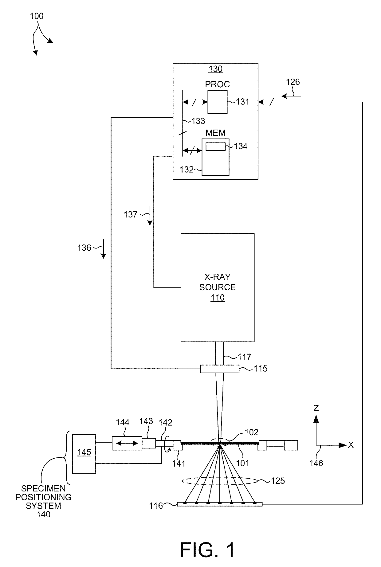
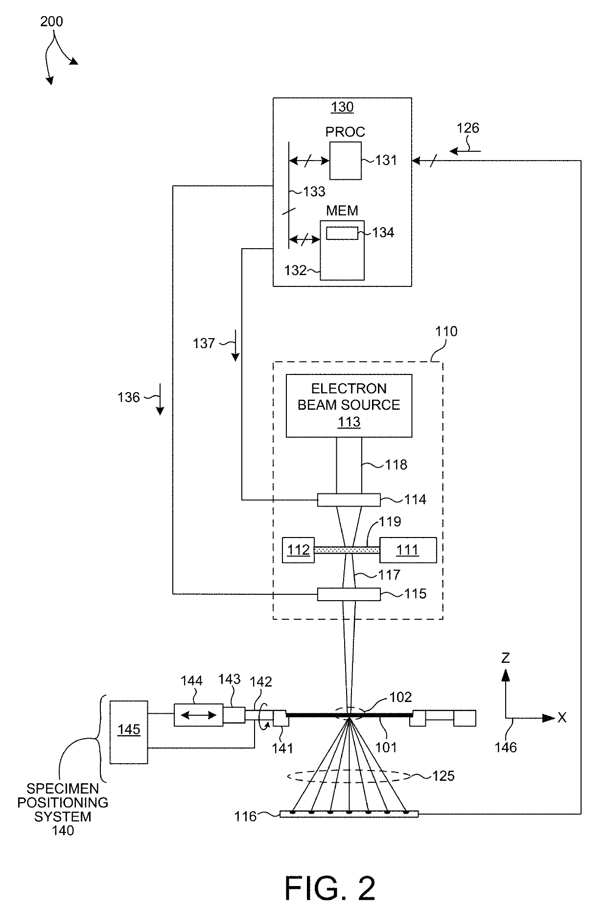
[0032]Methods and systems for characterizing dimensions and material properties of high aspect ratio, vertically manufactured devices using transmission, small-angle x-ray scattering (T-SAXS) techniques are described herein. Such systems and techniques are employed to measure structural and material characteristics associated with different semiconductor fabrication processes. In some examples, T-SAXS is employed to measure critical dimensions, thicknesses, overlay, and material properties of high aspect ratio semiconductor structures including, but not limited to, spin transfer torque random access memory (STT-RAM), three dimensional NAND memory (3D-NAND) or vertical NAND memory (V-NAND), dynamic random access memory (DRAM), three dimensional FLASH memory (3D-FLASH), resistive random access memory (Re-RAM), and phase...


PUM

PropertyMeasurementUnit
depthaaaaaaaaaa
roughnessaaaaaaaaaa
aspect ratioaaaaaaaaaa

Abstract

Methods and systems for characterizing dimensions and material properties of high aspect ratio, vertically manufactured devices using transmission, small-angle x-ray scattering (T-SAXS) techniques are described herein. Exemplary structures include spin transfer torque random access memory (STT-RAM), vertical NAND memory (V-NAND), dynamic random access memory (DRAM), three dimensional FLASH memory (3D-FLASH), resistive random access memory (Re-RAM), and PC-RAM. In one aspect, T-SAXS measurements are performed at a number of different orientations that are more densely concentrated near the normal incidence angle and less densely concentrated at orientations that are further from the normal incidence angle. In a further aspect, T-SAXS measurement data is used to generate an image of a measured structure based on the measured intensities of the detected diffraction orders. In another further aspect, a metrology system is configured to generate models for combined x-ray and optical measurement analysis.

Description

CROSS REFERENCE TO RELATED APPLICATION[0001]The present application for patent claims priority under 35 U.S.C. § 119 from U.S. provisional patent application Ser. No. 62 / 266,447, entitled “X-ray Scattering for Vertically Manufactured Devices,” filed Dec. 11, 2015, the subject matter of which is incorporated herein by reference in its entirety.TECHNICAL FIELD[0002]The described embodiments relate to metrology systems and methods, and more particularly to methods and systems for improved measurement accuracy.BACKGROUND INFORMATION[0003]Semiconductor devices such as logic and memory devices are typically fabricated by a sequence of processing steps applied to a specimen. The various features and multiple structural levels of the semiconductor devices are formed by these processing steps. For example, lithography among others is one semiconductor fabrication process that involves generating a pattern on a semiconductor wafer. Additional examples of semiconductor fabrication processes in...

Claims


Application Information

Patent Timeline
Patent Type & Authority Patents(United States)
IPC IPC(8): G01B15/02G01N23/201G01N23/20G01N23/2055
CPCG01B15/02G01N23/2055G01N23/201G01B2210/56G01N23/207G01N23/083G03F7/7085H01L22/12H01L22/24
Inventor DZIURA, THADDEUS GERARDGELLINEAU, ANTONIO ARIONSHCHEGROV, ANDREI V.
Owner KLA CORP
Why Eureka
Try Eureka