Quantum processing apparatus and a method of operating a quantum processing apparatus

a quantum processing and quantum processing technology, applied in the direction of superconductor details, superconductor devices, instruments, etc., can solve the problems of exponential decay of exchange interactions between electrons, the trend is now reaching a limit, and the difficulty in making current functional units (such as mosfets) any smaller without affecting their operation, etc., to achieve the effect of reducing the precision requirements of fabrication and accuracy in donor placemen

Active Publication Date: 2020-01-07
NEWSOUTH INNOVATIONS PTY LTD
View PDF7 Cites 31 Cited by
  • Summary
  • Abstract
  • Description
  • Claims
  • Application Information

AI Technical Summary

Benefits of technology

[0008]Embodiments of the invention propose a method to manipulate spin qubits with electric fields. The qubits manipulated in accordance with the method can be separated by hundreds of nanometres while preserving coupling capabilities. This substantially relaxes the precision requirements for fabrication. Advantageously, the schemes are compatible with the accuracy in donor placement achieved with ion implantation, as well as with scanning tunnelling microscope lithography.

Problems solved by technology

This trend is now reaching a limit, however, as it is difficult to make the current functional units (such as MOSFETs) any smaller without affecting their operation.
One of the problems related to this model is that the exchange interaction between electrons decays exponentially with donor separation and is highly dependent on the precise placement of the donors within a single lattice site, due to the oscillatory profile of the electron wave-function.
Such a level of precision makes the fabrication of the architecture very challenging, as discussed for example in U.S. Pat. No. 7,547,648 (Ruess et al.).
However, the limited coherence time and the associated fidelity of the quantum state in these systems represent a significant hurdle to application of quantum dots in a quantum processor.
More importantly, these materials suffer from problems with fidelity and dephasing time due to the presence of nuclear spins that are inherent to the GaAs crystal lattice.
These qubits however have a macroscopic size (hundreds of micrometres scale) which prevents architectures from being fabricated with a large number of qubits within a small chip size.
The large size, combined with the operation a GHz frequencies, can pose challenges in controlling the electromagnetic modes of a large number of qubits hosted in a cavity wider than the wavelength of the electromagnetic fields.

Method used


Image

  • Quantum processing apparatus and a method of operating a quantum processing apparatus
  • Quantum processing apparatus and a method of operating a quantum processing apparatus
  • Quantum processing apparatus and a method of operating a quantum processing apparatus

Examples


Embodiment Construction

[0112]In the following description a method for operating a processing element or a pair of processing elements in accordance with embodiments is described.

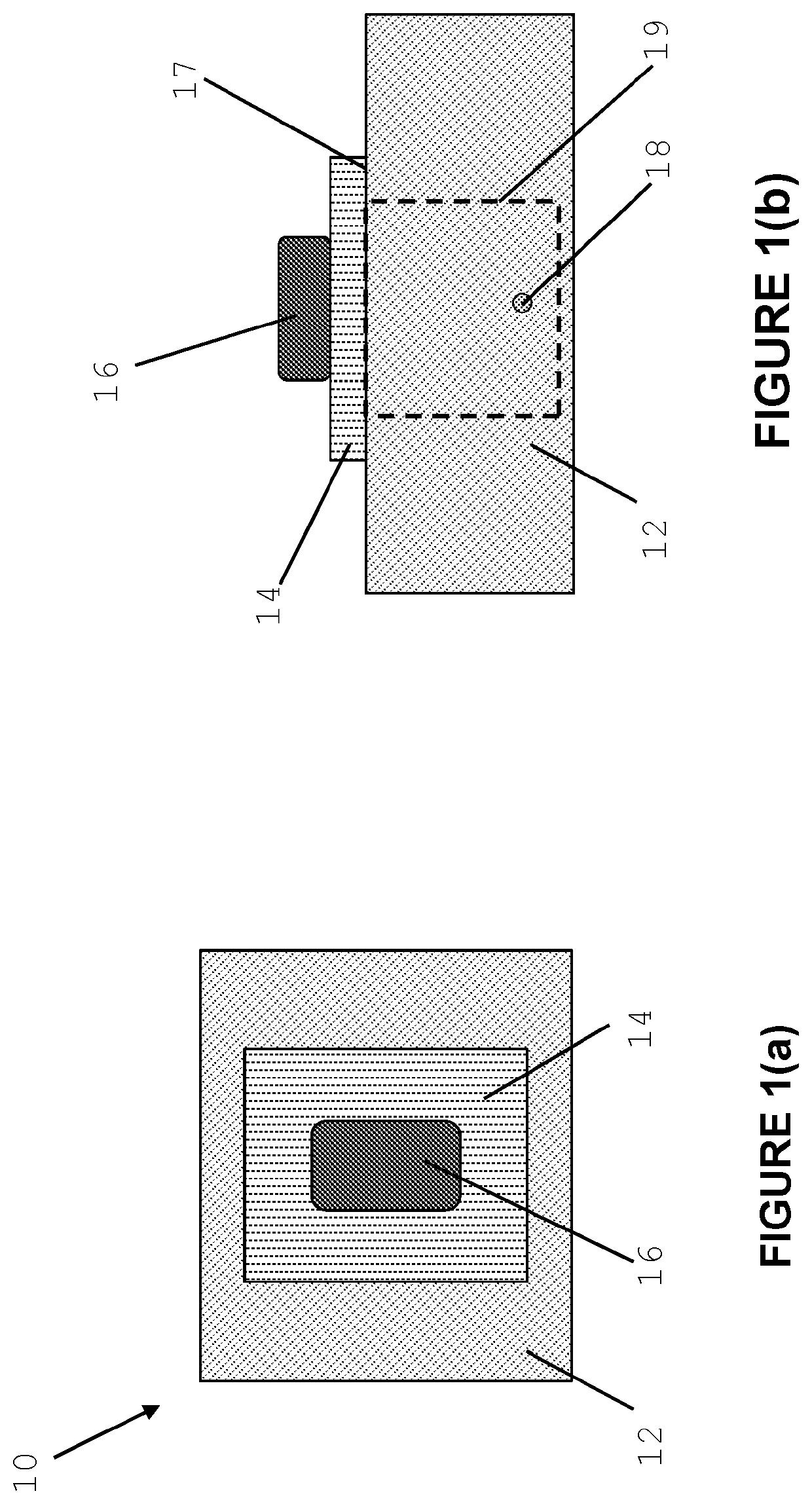
[0113]Referring to FIG. 1, there is shown a processing element 10 which can be operated using a method in accordance with embodiments. FIG. 1(a) is a top view of the processing element and FIG. 1(b) is a side cross-section. The processing element 10 may be used as a qubit element for a quantum computer comprising a plurality of these processing elements. Processing element 10 comprises a semiconductor substrate 12 and a dielectric 14, in this example being 28silicon and silicon dioxide respectively and forming a Si / SiO2 interface 17. A donor atom 18 is located within the substrate 12 inside region 19 under gate 16. The donor can be introduced into the substrate using nano-fabrication techniques, such the hydrogen lithography provided by scanning-tunneling-microscopes, or the industry-standard ion implantation techniques. Processi...


PUM

PropertyMeasurementUnit
frequencyaaaaaaaaaa
magnetic fieldaaaaaaaaaa
frequencyaaaaaaaaaa

Abstract

The present disclosure provides a method of operation of a quantum processing element and an advanced processing apparatus comprising a plurality of quantum processing elements operated in accordance with the method. Embodiments of the methods disclosed allow using the quantum properties of an MOS structure and a donor atom embedded in the semiconductor to implement electron and nuclear spin qubits and provide multi-qubit coupling, including coupling at longer distances facilitated by a resonator.

Description

FIELD OF THE INVENTION[0001]The present invention relates to a method of operation of a quantum processing element and an advanced processing apparatus comprising a plurality of quantum processing elements operated in accordance with the method.BACKGROUND OF THE INVENTION[0002]The power and capacity of computing components such as microprocessors and memory circuits has been increasing for the last 50 years, as the size of the functional units, such as transistors, has been decreasing. This trend is now reaching a limit, however, as it is difficult to make the current functional units (such as MOSFETs) any smaller without affecting their operation.[0003]The technology employed to manufacture conventional silicon integrated circuits is today well established. Current microprocessors feature several hundreds of millions of transistors which are manufactured in high throughput lines.[0004]Developments are ongoing to implement new types of advanced processing apparatuses that can implem...

Claims


Application Information

Patent Timeline
Patent Type & Authority Patents(United States)
IPC IPC(8): G06N10/00B82Y10/00H03K19/08G01N24/10G01R33/60H01L27/18H01L39/02H01L39/22
CPCG01R33/60H03K19/08B82Y10/00H01L39/025H01L39/223G01N24/10G06N10/00H01L27/18H10N60/12H10N60/805H10N69/00
Inventor MORELLO, ANDREATOSI, GUILHERMEMOHIYADDIN, FAHD A.
Owner NEWSOUTH INNOVATIONS PTY LTD
Why Eureka
Try Eureka