Wireless power transfer system with open loop reactance matching circuitry

a technology of reactance matching and wireless power transfer, applied in the field of power electronics, can solve the problems of affecting the performance of the controller, high driving voltage, and inability to design a robust close-loop controller, so as to improve coupling, reduce the effect of magnetizing inductance, and improve the coupling

Active Publication Date: 2021-08-24
GLOWOLT INC
View PDF10 Cites 0 Cited by
  • Summary
  • Abstract
  • Description
  • Claims
  • Application Information

AI Technical Summary

Benefits of technology

[0006]In one embodiment, power is transferred wirelessly via a transformer effect or magnetic coupling between two coupled coils. In this embodiment, lack of an iron core and a large gap between the primary and secondary coils will cause loose coupling with low magnetizing inductance between transmitter and receiver coils. To improve the coupling between the transmitter and receiver coils, an operational frequency needs to be significantly increased. Increasing the operational frequency has adverse effects, such as increasing the leakage reactance of the transmitter and receiver coils, and increasing the resistive losses due to the skin effect. To compensate for leakage reactance of the transmitter and receiver coils, several novel techniques are employed. First, series capacitors are provided in a distributed manner to compensate a major portion of the transmitter coil reactance. By distributing the capacitors, an improved voltage profile and lower capacitor losses are achieved. Second, precise reactance matching is provided by an Open Loop Reactance Matching (OLRM) control circuit. A voltage source converter with a capacitive DC-link is used in series with the source and switched with a 90-degrees lead or lag phase shift in relation to the source voltage signal. Third, switched capacitors are used in series with the voltage source converter to alleviate the amount of required semiconductor switches, and to reduce stress on the voltage source converter. The switched capacitors switch OFF and ON with respect to the DC link voltage value.
[0007]To reduce resistive losses due to the skin effect, a transmitter source is operated as a current source with constant magnitude, regardless of load condition. The current is low enough to reduce transmitter losses while still providing enough magnetic flux for wireless power transfer. In the absence of a receiver, the voltage across the current source is low, and is equal to the resistance of the transmitter conductor multiplied by the transmitter current. This results from the perfect reactance matching provided by the novel OLRM control circuit that compensates for all the reactance of the transmitter circuit. When a receiver circuit with resistive load couples with a portion of the transmitter circuit, the reactance of that portion is replaced by the resistance of the load and does not become compensated by the reactance matching scheme. As such, the voltage across the current source increases to keep the current magnitude through the transmitter circuit constant. This is effectively equivalent to transferring power from the source to the receiver circuit load since power is equal to voltage multiplied by current. In this case, power transfers through voltage rather than through current. Losses of the transmitter will remain nearly constant and similar to a zero load condition because the transmitter current is maintained constant. In some embodiments, a DC-to-DC buck-boost power converter circuit or transformer is used between the load and receiver circuit for adjusting equivalent resistance under different loading conditions. In addition, a Litz wire, aluminum, or copper foil is used to reduce the skin effect losses.
[0008]In one embodiment, a wireless power transfer system has one or more transmitter circuits coupled to a conductor. A system operational frequency is fixed and does not need any adjustment under varying loading conditions. Any number of receiver circuits may receive power simultaneously from the one or more transmitter circuits. In this embodiment, transmitter and receiver coils do not need to be planar spiral inductors, and, depending on a magnitude of the system operational frequency, only one turn can be used at the transmitter circuit. Distributed series capacitors are used to compensate a major portion of a transmitter inductance. The distributed series capacitors provide a better voltage profile across the conductor, which is important for insulator design and reduces capacitor losses that would otherwise result at high voltages.
[0009]To reduce undesirable skin effect, eddy current, proximity effect, and capacitor losses, the transmitter circuit is designed with at least one of several novel features. In one example, a conductor is provided having a Litz wire and multilayer ceramic capacitors coupled in series. The multilayer ceramic capacitors are distributed throughout the conductor and compensate the conductor. In another example, a conductor is provided having a plurality of sections of copper or aluminum foil. Each section is isolated from the other by a dielectric material. The common area between each section creates the required distributed capacitors for compensating the conductor. In still another example, a conductor is provided having a plurality of sections of copper or aluminum tubes. Each section is isolated from the other by a dielectric material. The common area between each section creates the required distributed capacitors for compensating the conductor.
[0010]Reactance matching is obtained by a voltage source converter with a capacitive DC link. The voltage source converter is controlled to switch with 90-degrees lead or lag in relation to the source voltage signal. Either a half-bridge or full-bridge inverter is used as the voltage source converter. A phase-shifted full-bridge DC-to-AC inverter is used to reduce the switching losses due to Zero Voltage Switching (ZVS). Fast switches such as Silicon Carbide (SiC) or Gallium Nitride (GaN) are used to reduce switching losses. Switched capacitors are used in series with the voltage source converter to alleviate the amount of required semiconductor switches and to reduce stress on the voltage source converter. The switched capacitors switch OFF or ON with respect to the DC-link voltage level. If the DC-link voltage level is too high, then switched capacitors will go online to reduce the DC-link voltage. If, on the other hand, the DC-link voltage level is too low, then the switched capacitors will go offline to maintain precise reactance matching.
[0013]The novel wireless power transfer systems are bidirectional and power is transferable from the receiver circuits to the transmitter circuits. The wireless power transfer systems have minimal impact on foreign conductive objects due to the low resistance path of these objects. The wireless power transfer systems are usable to wirelessly transfer power to home appliances and all electronic devices. In addition, the wireless power transfer systems are usable to wirelessly transfer power to all moving vehicles operated in everyday life, including vehicles, buses, high occupancy passenger vehicles, shuttles, commercial vehicles, and delivery vehicles operating on roads. In one embodiment, various wireless power transfer systems are provided but are not synchronized. In this case, traveling vehicles momentarily lose energy while moving from one loop (transmitter conductor) of a wireless power transfer system to another loop of a different wireless power transfer system. In another embodiment, one loop extends across a roadway and is synchronized with various transmitter circuits. In this example, the current sources at the various locations of the loops are synchronized. The synchronization is done in one example via GPS signals or via current through a power line. This embodiment provides more reliability and vehicles will not lose energy while within the loop. To control the current sources, a decentralized control scheme such as a droop controller is utilized.

Problems solved by technology

Reactance matching circuits with all passive elements are typically not precise, and, especially in the case of high reactance values, even the slightest error in the matching circuit will result in a high driving voltage which for some cases may not be practical.
In high frequency and low current applications, designing a robust close loop controller is nontrivial and performance of the controller is affected by the accuracy of the sensors and digital controller.
In this embodiment, lack of an iron core and a large gap between the primary and secondary coils will cause loose coupling with low magnetizing inductance between transmitter and receiver coils.
Increasing the operational frequency has adverse effects, such as increasing the leakage reactance of the transmitter and receiver coils, and increasing the resistive losses due to the skin effect.
When a receiver circuit with a resistive load couples with a portion of the transmitter circuit, then a reactance of that portion is replaced by the resistance of the load and is not compensated by the reactance matching functionality.

Method used


Image

  • Wireless power transfer system with open loop reactance matching circuitry
  • Wireless power transfer system with open loop reactance matching circuitry
  • Wireless power transfer system with open loop reactance matching circuitry

Examples


Embodiment Construction

[0038]Reference will now be made in detail to some embodiments of the invention, examples of which are illustrated in the accompanying drawings.

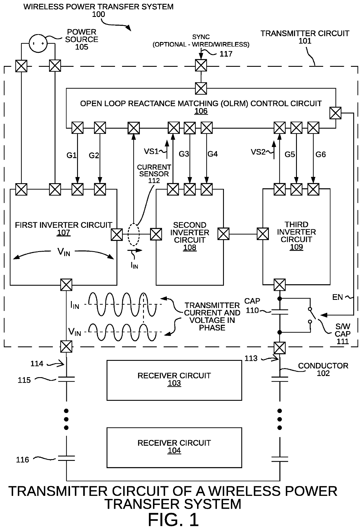
[0039]FIG. 1 is a diagram of a wireless power transfer system 100. The wireless power transfer system 100 comprises a transmitter circuit 101, a conductor 102, and receiver circuits 103 and 104, and a power source 105. In this example, the power source 105 is a Direct Current (DC) source that supplies a DC voltage to the transmitter circuit 101. In other embodiments, the power source 105 is an Alternating Current (AC) source that supplies an AC voltage to the transmitter circuit 101. The transmitter circuit 101 supplies the receiver circuits 103 and 104 wirelessly via the conductor 102. The transmitter circuit 101 comprises an Open Loop Reactance Matching (OLRM) control circuit 106, a first inverter circuit 107, a second inverter circuit 108, a third inverter circuit 109, a capacitor 110, a switch 111, and a current sense circuit 112. The fi...


PUM

PropertyMeasurementUnit
frequencyaaaaaaaaaa
voltageaaaaaaaaaa
DC voltageaaaaaaaaaa

Abstract

A system includes a power source, a transmitter circuit, a conductor, and a receiver circuit. The transmitter circuit is supplied by the power source and wirelessly supplies the receiver circuit via the conductor. The conductor includes a plurality of distributed capacitances coupled in series with the conductor. The receiver circuit includes a primary coil and a secondary coil. The primary coil has at least two turns and includes a plurality of distributed capacitances. The transmitter circuit includes an Open Loop Reactance Matching (OLRM) control circuit, a first inverter, a second inverter, and a third inverter. The OLRM control circuit controls the first inverter to generate a high frequency AC voltage to be supplied to the conductor. During wireless power transfer, the OLRM control circuit performs reactance matching by controlling the second and third inverters to maintain the transmitter voltage and current in phase without requiring any feedback sensing.

Description

CROSS REFERENCE TO RELATED APPLICATIONS[0001]This application claims the benefit under 35 U.S.C. § 119 from U.S. Provisional Patent Application Ser. No. 62 / 909,854, entitled “Open Loop Reactance Matching (OLRM) and Application for Wireless Power Transfer,” filed on Oct. 3, 2019, the subject matter of which is incorporated herein by reference.TECHNICAL FIELD[0002]The present invention relates generally to power electronics, and more specifically to wireless power transfer circuitry.BACKGROUND INFORMATION[0003]Wireless power transfer systems provide transmission of electrical energy without wired links. In a typical wireless power transfer system, a transmitter receives electrical energy from a power source and generates a magnetic field. The magnetic field wirelessly transmits power to a receiver device across space. The receiver device receives the wireless power transmission and supplies an electrical load. Wireless power transmission eliminates wired connections and is more conven...

Claims


Application Information

Patent Timeline
Patent Type & Authority Patents(United States)
IPC IPC(8): H02J50/05H02J50/12H01F38/14H02J50/40H02M7/5387H01F27/24
CPCH02J50/05H01F38/14H02J50/12H02J50/40H02M7/53871H01F27/24H02M7/4835H02J50/005H02J50/402H03F3/21H03H11/28
Inventor KHALILINIA, HAMED
Owner GLOWOLT INC
Why Eureka
Try Eureka