Switch device, storage apparatus, and memory system

a technology of switch device and storage device, applied in the direction of digital storage, semiconductor device, instrument, etc., can solve the problems of large floor area per unit cell and difficult increase in capacity

Active Publication Date: 2021-11-23
SONY SEMICON SOLUTIONS CORP
View PDF29 Cites 0 Cited by
  • Summary
  • Abstract
  • Description
  • Claims
  • Application Information

AI Technical Summary

Benefits of technology

[0011]It is desirable to provide a switch device that makes it possible to improve stability of the threshold voltage, and a storage apparatus and a memory system each of which includes the switch device.
[0015]In the switch device according to the embodiment of the present disclosure, the storage apparatus according to the embodiment of the present disclosure, and the memory system according to the embodiment of the present disclosure, the switch layer includes one or more kinds of chalcogen elements selected from tellurium (Te), selenium (Se), and sulfur (S), one or more kinds of first elements selected from phosphorus (P) and arsenic (As), and one or both of one or more kinds of second elements selected from boron (B) and carbon (C) and one or more kinds of third elements selected from aluminum (Al), gallium (Ga), and indium (In). This makes it possible to stabilize an amorphous structure of the switch layer and reduce fluctuations in threshold voltage.
[0016]According to the switch device according to the embodiment of the present disclosure, the storage apparatus according to the embodiment of the present disclosure, and the memory system according to the embodiment of the present disclosure, the switch layer is formed with use of the above-described elements, which stabilizes the amorphous structure of the switch layer. This makes it possible to improve stability of the threshold voltage.

Problems solved by technology

In existing resistance change memories using an access transistor, however, a floor area per unit cell is large.
Therefore, the increase in capacity is not easy even if miniaturization is performed under the same design rule, as compared with, for example, flash memories such as an NAND flash memory.

Method used


Image

  • Switch device, storage apparatus, and memory system
  • Switch device, storage apparatus, and memory system
  • Switch device, storage apparatus, and memory system

Examples


modification example 2 (

4-2. Modification Example 2 (an example of a memory cell array having a three-dimensional configuration)

5. APPLICATION EXAMPLE (DATA STORAGE SYSTEM)

6. EXAMPLES

first embodiment

(1-1. Configuration of Switch Device)

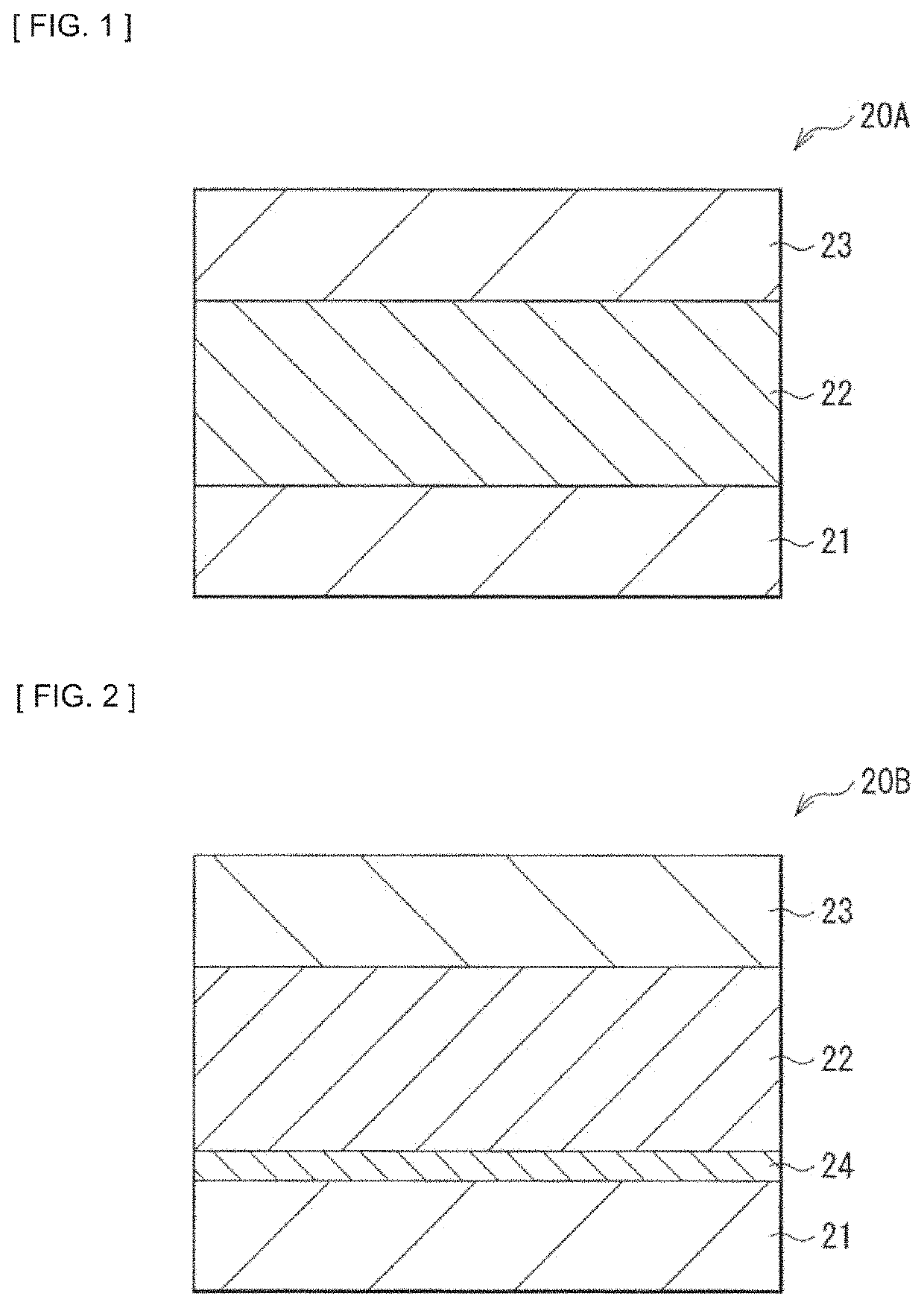
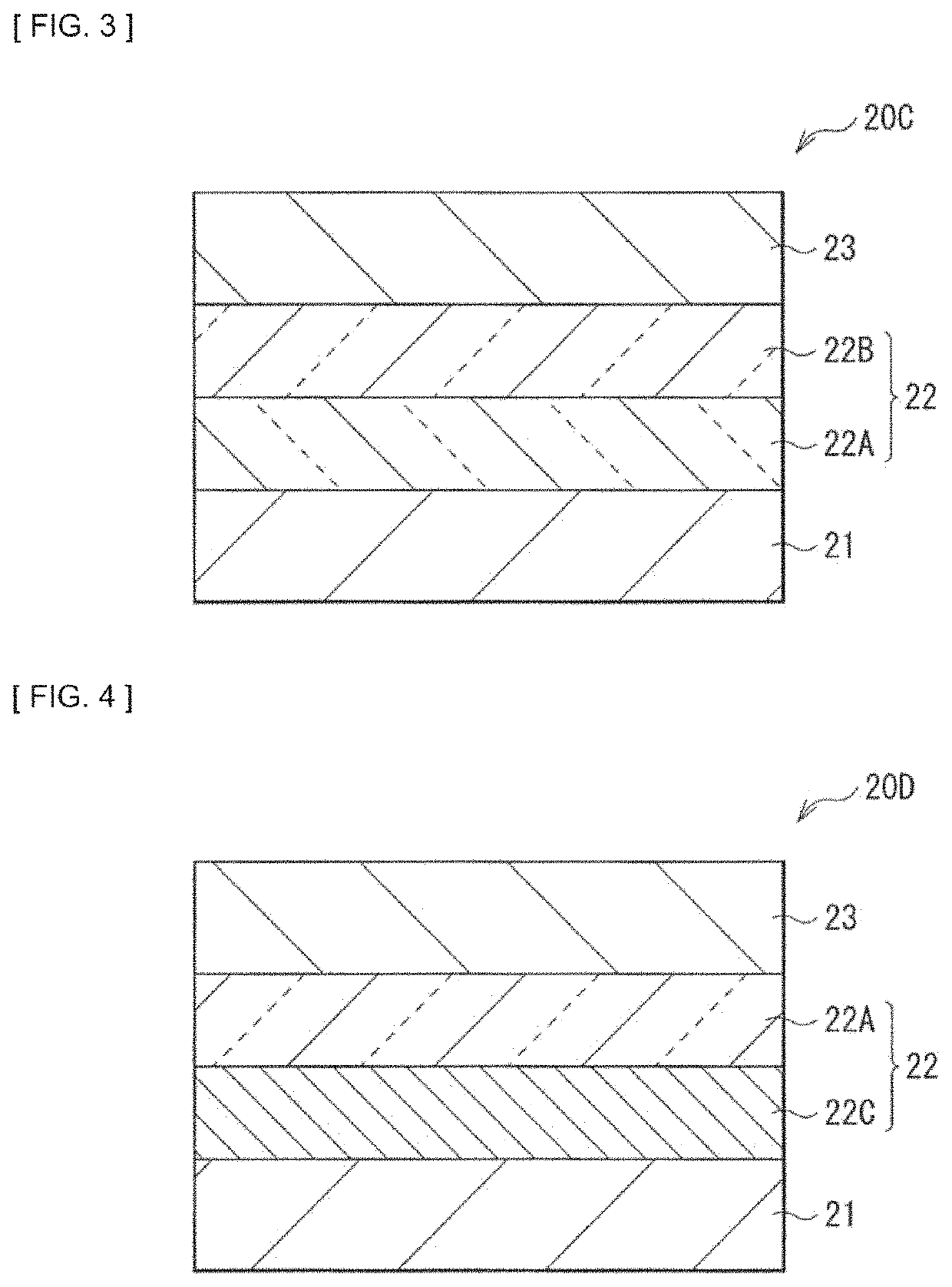
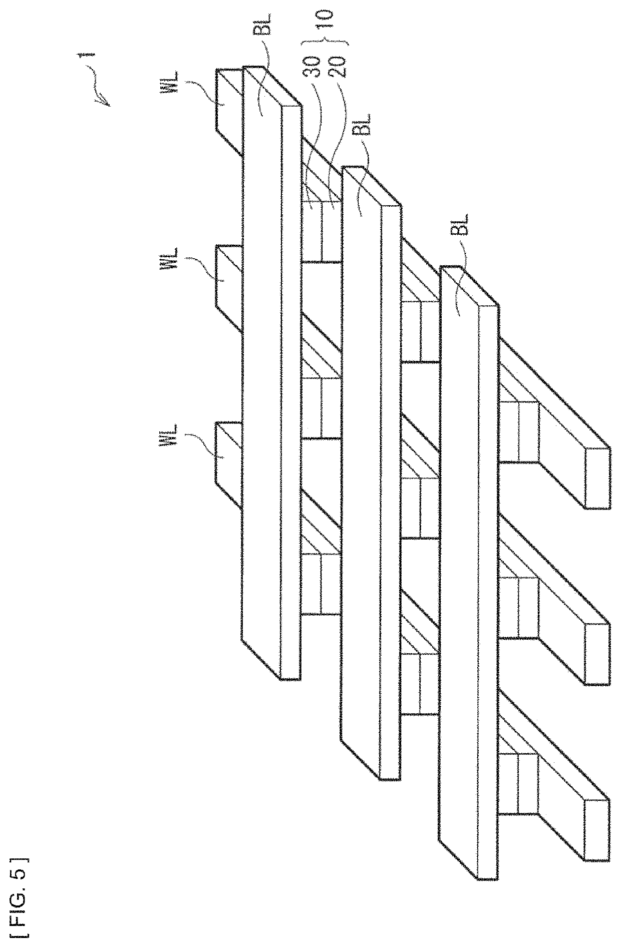
[0044]FIG. 1 illustrates an example of a cross-sectional configuration of a switch device (a switch device 20A) according to a first embodiment of the present disclosure. The switch device 20A selectively operates any of a plurality of storage devices (memory devices 30; FIG. 5) arranged in a memory cell array 1 having a so-called cross point array structure illustrated in FIG. 5, for example. The switch device 20A (a switch device 20; FIG. 5) is coupled in series to the memory device 30 (specifically, a memory layer 31), and includes a lower electrode 21 (a first electrode), a switch layer 22, and an upper electrode 23 (a second electrode) in this order.

[0045]The lower electrode 21 includes a wiring material used for a semiconductor process. Examples of the wiring material include tungsten (W), tungsten nitride (WN), titanium nitride (TiN), carbon (C), copper (Cu), aluminum (Al), molybdenum (Mo), tantalum (Ta), tantalum nitride (TaN), silicide, ...

second embodiment

(2-1 Configuration of Switch Device)

[0093]FIG. 14 illustrates an example of a cross-sectional configuration of a switch device (a switch device 50) according to the second embodiment of the present disclosure. The switch device 50 selectively operates any of a plurality of storage devices (memory devices 30) arranged in the memory cell array 1 having a so-called cross point array structure illustrated in FIG. 5, for example, as with the switch device 20 (or 20A, 20B, 20C, or 20D) according to the foregoing first embodiment. The switch device 50 includes the lower electrode 21 (the first electrode), a switch layer 52, and the upper electrode 23 (the second electrode) in this order.

[0094]The lower electrode 21 and the upper electrode 23 each include any of the materials described in the foregoing first embodiment. Examples of the materials include tungsten (W), tungsten nitride (WN), titanium nitride (TiN), carbon (C), copper (Cu), aluminum (Al), molybdenum (Mo), tantalum (Ta), tantal...


PUM


Abstract

A switch device includes: a first electrode; a second electrode opposed to the first electrode; and a switch layer provided between the first electrode and the second electrode, and the switch layer includes one or more kinds of chalcogen elements selected from tellurium (Te), selenium (Se), and sulfur (S) and one or more kinds of first elements selected from phosphorus (P) and arsenic (As), and further includes one or both of one or more kinds of second elements selected from boron (B) and carbon (C) and one or more kinds of third elements selected from aluminum (Al), gallium (Ga), and indium (In).

Description

CROSS REFERENCE TO RELATED APPLICATIONS[0001]This application is a U.S. National Phase of International Patent Application No. PCT / JP2017 / 032811 filed on Sep. 12, 2017, which claims priority benefit of Japanese Patent Application No. JP 2016-196669 filed in the Japan Patent Office on Oct. 4, 2016 and also claims priority benefit of Japanese Patent Application No. JP 2017-008138 filed in the Japan Patent Office on Jan. 20, 2017. Each of the above-referenced applications is hereby incorporated herein by reference in its entirety.TECHNICAL FIELD[0002]The present disclosure relates to a switch device including a chalcogenide layer between electrodes, and to a storage apparatus and a memory system each of which includes the switch device.BACKGROUND ART[0003]In recent years, an increase in capacity is demanded for data storage non-volatile memories represented by resistance change memories such as a ReRAM (resistance random access memory) and a PRAM (Phase-Change Random Access Memory) (re...

Claims


Application Information

Patent Timeline
Patent Type & Authority Patents(United States)
IPC IPC(8): H01L45/00H01L27/24H01L27/22H01L21/8239G11C13/00H01L27/105
CPCH01L45/141G11C13/0011H01L21/8239H01L27/105H01L27/224H01L27/249H01L27/2427H01L27/2463H01L27/2481H01L45/06H01L45/08H01L45/1233H01L45/1266H01L45/145H01L45/147G11C13/0004G11C2213/15G11C2213/71G11C11/161G11C17/16G11C17/165G11C13/0002H10B63/845H10B63/80H10N70/24H10N70/8416H10N70/882H10N70/883H10N70/826H10B99/00H10N70/801H10N70/881H10N70/231H10N99/00H10B61/10H10B63/24H10B63/84H10N70/8836
Inventor SEI, HIROAKIOHBA, KAZUHIROSONE, TAKEYUKINONOGUCHI, SEIJIIKARASHI, MINORU
Owner SONY SEMICON SOLUTIONS CORP
Why Eureka
Try Eureka