
Method of forming metal nitride film by chemical vapor deposition and method of forming metal contact and capacitor of semiconductor device using the same

a technology of metal nitride and chemical vapor deposition, which is applied in the direction of chemical vapor deposition coating, coating, capacitor, etc., can solve the problems of high-integration semiconductor devices that cannot be applied, the deposition temperature of 600.degree. c. or more exceeds the thermal budget and thermal stress limits of an underlayer

Inactive Publication Date: 2001-10-25
SAMSUNG ELECTRONICS CO LTD
View PDF0 Cites 294 Cited by
  • Summary
  • Abstract
  • Description
  • Claims
  • Application Information

AI Technical Summary

Benefits of technology

[0016] Another objective of the present invention is to provide a method of forming a metal contact having a barrier metal layer which has excellent step coverage even at a high deposition speed and a low temperature, low impurity concentration, and low resistivity, by applying the metal nitride film formation method to a metal contact of a semiconductor device.
[0017] Still another objective of the present invention is to provide a method of forming a capacitor which gives excellent step coverage, low impurity concentration and low resistivity, using the metal nitride film formation method.
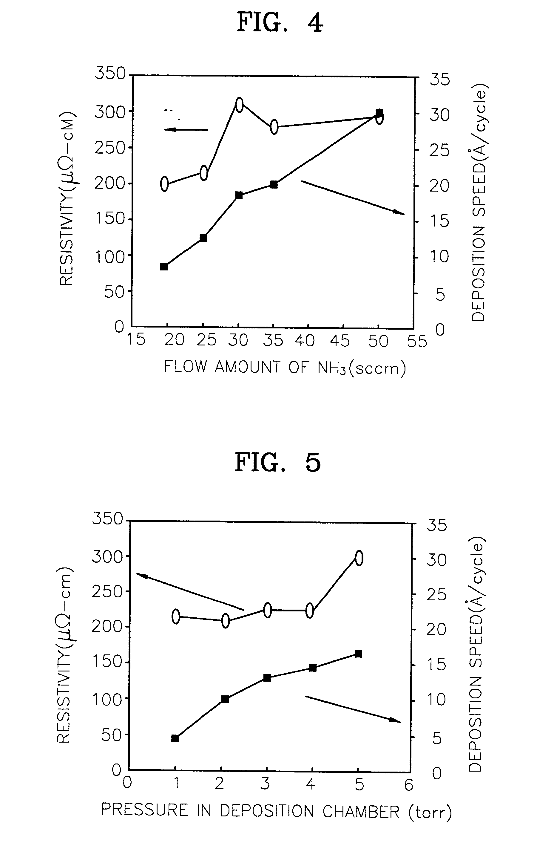
[0039] According to the present invention, a metal nitride film having low resistivity of 200.mu..OMEGA.-cm or less and a low content of Cl can be obtained even with excellent step coverage. Also, a CVD-metal nitride film can be formed at a temperature of 500.degree. C. or less even at a deposition speed of about 20 A / cycle, so that the deposition speed of the present invention is higher than that of a metal nitride film formation method using ALE having a growth speed of 0.25 A / cycle. A capacitor, in which a metal nitride film formed by the method according to the present invention is used as a lower and / or upper conductive layer, has excellent step coverage and excellent leakage current characteristics.

Problems solved by technology

However, when the metal nitride film such as TiN is fabricated by sputtering, its application to highly integrated semiconductor devices is not appropriate, due to low step coverage.
Thus, voids are likely to be generated upon subsequent tungsten deposition.
However, a deposition temperature of 600.degree. C. or more exceeds thermal budget and thermal stress limits which an underlayer can withstand.
In particular, when the metal nitride film is deposited on an Si contact or a via contact with an Al underlayer, a deposition temperature of 480.degree. C. or lower is required, so that a high temperature CVD-metal nitride film process cannot be used.
A low temperature deposition CVD-metal nitride film process is possible, by adding MH (methylhydrazine, (CH.sub.3)HNNH.sub.2) to the metal source such as TiCl.sub.4, but this method has a defect in that step coverage is decreased to 70% or lower.
However, the MOCVD-metal nitride film contains a lot of carbon (C) as impurities, giving high resistivity, and has inferior step coverage of 70% or less.
However, the ALE grows the metal nitride film in units of an atomic layer using only chemical absorption, and the deposition speed (0.25 A / cycle or less) is too slow to apply the ALE to mass production.
Semiconductor capacitors, which use the TiN film as an electrode, also have the above-described problems.
Hence, the shape of the semiconductor capacitor is so complicated that it is critical to guarantee step coverage of deposited materials as its electrode.
However, as described above, the CVDed TiN film provokes corrosion of metal wiring and gives high resistivity, due to a high concentration of Cl, resulting in a degradation in the leakage current characteristics of a capacitor.

Method used


Image

  • Method of forming metal nitride film by chemical vapor deposition and method of forming metal contact and capacitor of semiconductor device using the same
  • Method of forming metal nitride film by chemical vapor deposition and method of forming metal contact and capacitor of semiconductor device using the same
  • Method of forming metal nitride film by chemical vapor deposition and method of forming metal contact and capacitor of semiconductor device using the same

Examples


Embodiment Construction

>

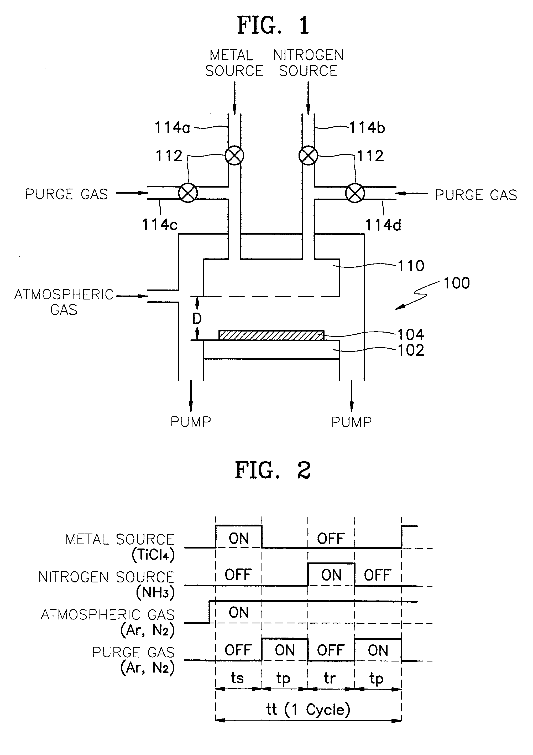
[0072] A TiN film is deposited by the cycles comprising the gas pulsing steps, under the following reaction conditions, on the semiconductor substrate 104 which is maintained at a temperature of 500.degree. C. or lower by the heater 102 of FIG. 1.

[0073] Deposition Conditions

[0074] object material: TiN

[0075] atmospheric gas: Ar

[0076] pressure in deposition chamber: 1-20Torr

[0077] metal source, nitrogen source: TiCl.sub.4, NH.sub.3

[0078] flow amount of TiCl.sub.4, pulsing time (t.sub.s) of TiCl.sub.4:1-5 sccm, 5 sec

[0079] flow amount of NH.sub.3, pulsing time (t.sub.r) of NH.sub.3: 5-30 sccm, 5 sec

[0080] purge gas, flow amount of purge gas, purge time (t.sub.p): Ar, 10-100 sccm, 10 sec

[0081] carrier gas, flow amount of carrier gas: Ar, 10-100 sccm

[0082] time (t.sub.t) for one cycle: 30 sec

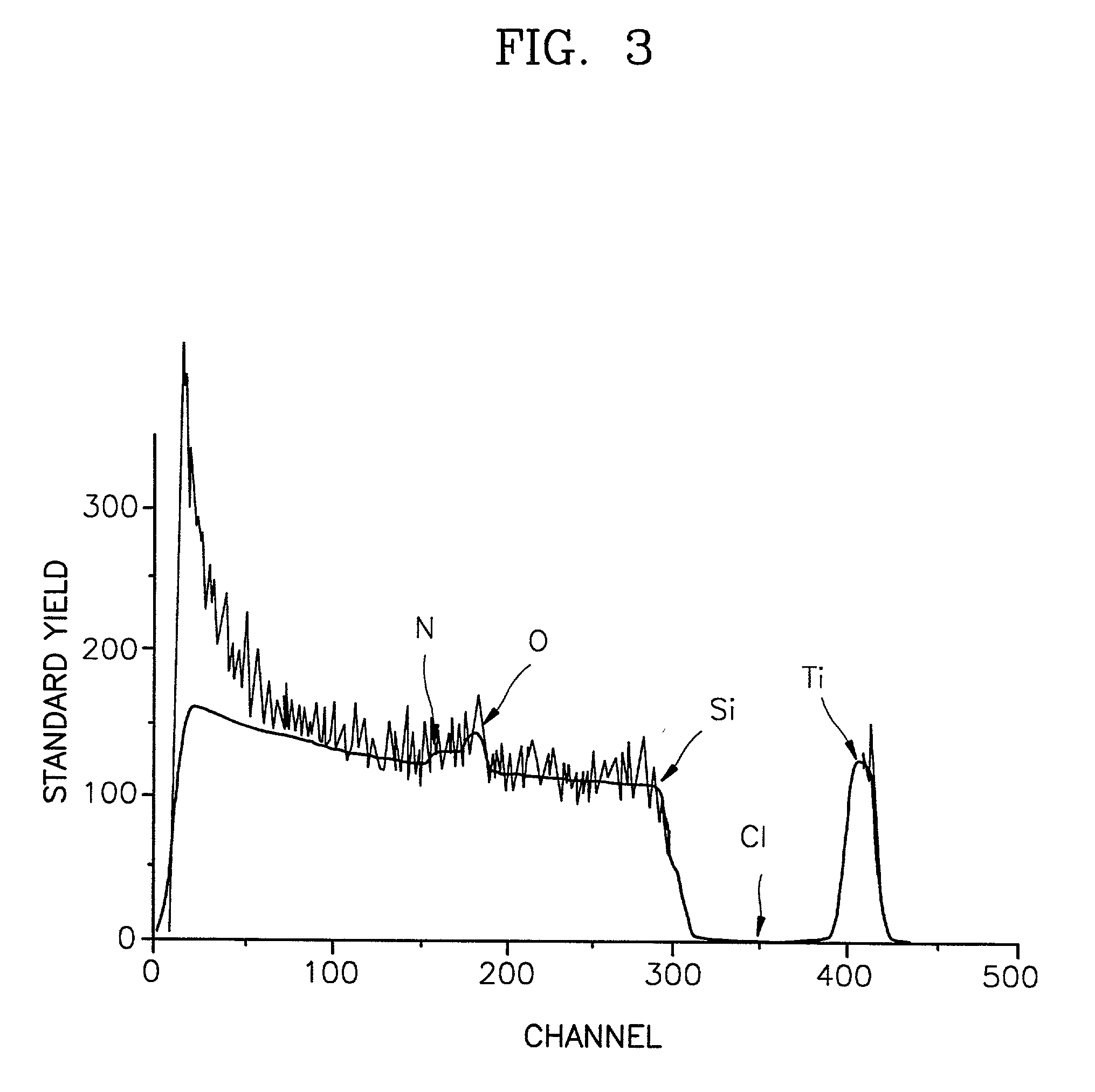
[0083] FIG. 3 shows the results of checking the state of the TiN thin film deposited on the semiconductor substrate 104 under the aforementioned conditions using an RBS method. In FIG. 3, a horizont...


PUM

PropertyMeasurementUnit
pressureaaaaaaaaaa
temperatureaaaaaaaaaa

Abstract

A method of forming a metal nitride film using chemical vapor deposition (CVD), and a method of forming a metal contact and a semiconductor capacitor of a semiconductor device using the same, are provided. The method of forming a metal nitride film using chemical vapor deposition (CVD) in which a metal source and a nitrogen source are used as a precursor, includes the steps of inserting a semiconductor substrate into a deposition chamber, flowing the metal source into the deposition chamber, removing the metal source remaining in the deposition chamber by cutting off the inflow of the metal source and flowing a purge gas into the deposition chamber, cutting off the purge gas and flowing the nitrogen source into the deposition chamber to react with the metal source adsorbed on the semiconductor substrate, and removing the nitrogen source remaining in the deposition chamber by cutting off the inflow of the nitrogen source and flowing the purge gas into the deposition chamber. Accordingly, the metal nitride film having low resistivity and a low content of Cl even with excellent step coverage can be formed at a temperature of 500° C. or lower, and a semiconductor capacitor having excellent leakage current characteristics can be manufactured. Also, a deposition speed, approximately 20 A / cycle, is suitable for mass production.

Description

[0001] This application is a continuation-in-part of U.S. patent application Ser. No. 09 / 156,724, filed Sep. 18, 1998, entitled METHOD OF FORMING METAL NITRIDE FILM CHEMICAL VAPOR DEPOSITION AND METHOD OF FORMING METAL CONTACT OF SEMICONDUCTOR DEVICE USING THE SAMEMETHOD OF FORMING METAL NITRIDE FILM CHEMICAL VAPOR DEPOSITION AND METHOD OF FORMING METAL CONTACT OF SEMICONDUCTOR DEVICE USING THE SAME.[0002] 1. Field of the Invention[0003] The present invention relates to a method of fabricating semiconductor devices, and more particularly, to a method of forming a metal nitride film by chemical vapor deposition (CVD) where a metal source and a nitrogen source are used as a precursor, and a method of forming a metal contact and a capacitor of a semiconductor device using the above method.[0004] 2. Description of the Related Art[0005] A barrier metal layer, which prevents mutual diffusion or chemical reaction between different materials, is indispensable to stabilize the contact interf...

Claims


Application Information

Patent Timeline
Patent Type & Authority Applications(United States)
IPC IPC(8): C23C16/04C23C16/34C23C16/44C23C16/455H01L21/02H01L21/285H01L21/768
CPCC23C16/34C23C16/45553H01L21/28562H01L21/76804H01L21/76843H01L28/91
Inventor LIM, HYUN-SEOKKANG, SANG-BOMJEON, IN-SANGCHOI, GIL-HEYUN
Owner SAMSUNG ELECTRONICS CO LTD
Learn More