Ceramic circuit board and method of manufacturing the same
a ceramic circuit board and ceramic technology, applied in the direction of printed circuit non-printed electric components association, insulating substrate metal adhesion improvement, semiconductor/solid-state device details, etc., can solve the problems of increasing the number of chipping flaws, unable to achieve good heat-radiating properties at all, and insufficient technical stage to cope with them. , to achieve the effect of reducing the anisotropy of surface roughness, high reliability and increased transverse strength of ceramic circuit boards
- Summary
- Abstract
- Description
- Claims
- Application Information
AI Technical Summary
Benefits of technology
Problems solved by technology
Method used
Image

Examples
examples 1-6
[0098] A material powder mixture was prepared by adding 5 wt % of Y.sub.2O.sub.3 (yttrium oxide) powder having an average grain size of 0.7 .mu.m and 1.5 wt % of Al.sub.2O.sub.3 (alumina) powder having an average grain size of 0.5 .mu.m as a sintering assistant agent, to silicon nitride material powder containing 1.3 wt % of oxygen, 0.15 wt % of impurity cationic elements and 97 wt % of a-phase silicon nitride, and having an average grain size of 0.55 .mu.m, followed by wet-mixing the materials in ethyl alcohol for 24 hours, and drying the mixture. After adding a predetermined amount of an organic binder and a solvent to the material powder mixture, the mixture was homogeneously mixed thereby to prepare a material slurry.
[0099] Next, the above material slurry was sheet-molded in accordance with a doctor blade method while an opening width of a blade and an extrusion rate of the material slurry extruded from the blade were controlled, thereby to prepare a number of sheet-shaped molde...
examples 7-12
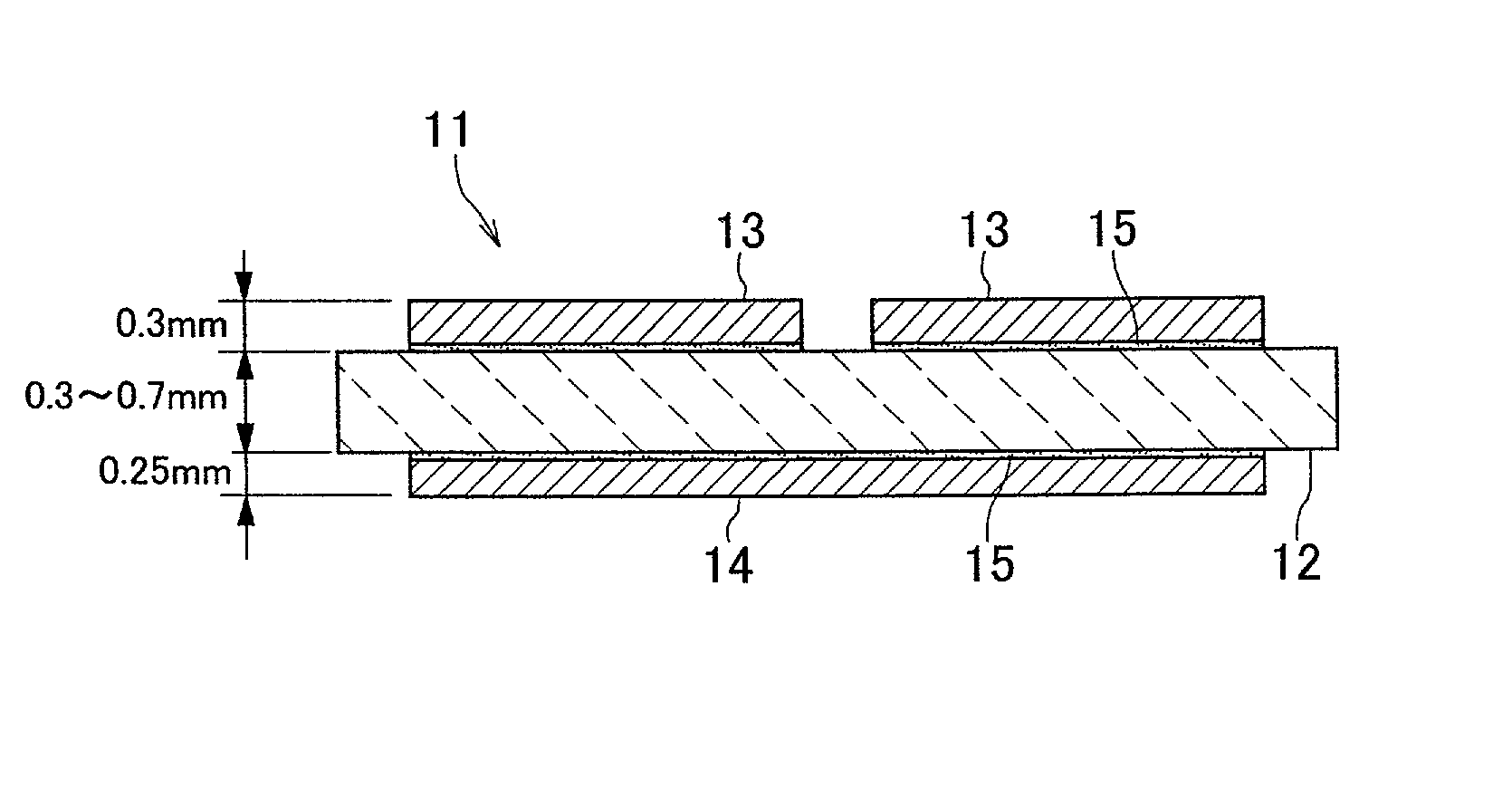
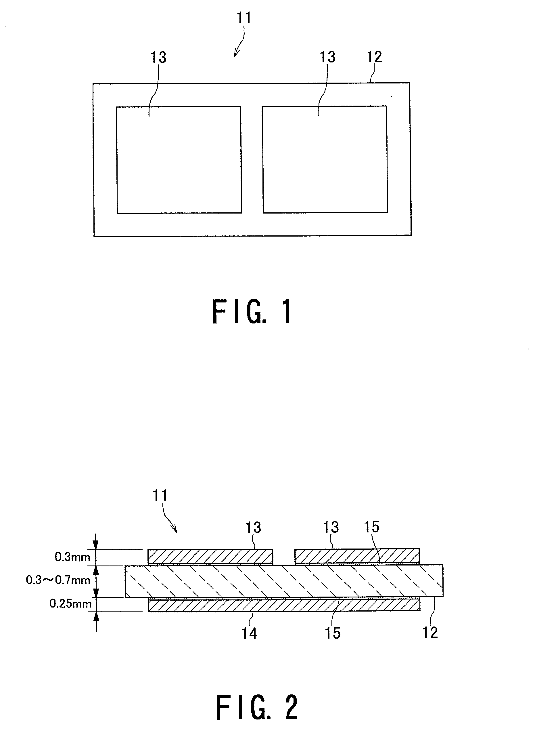
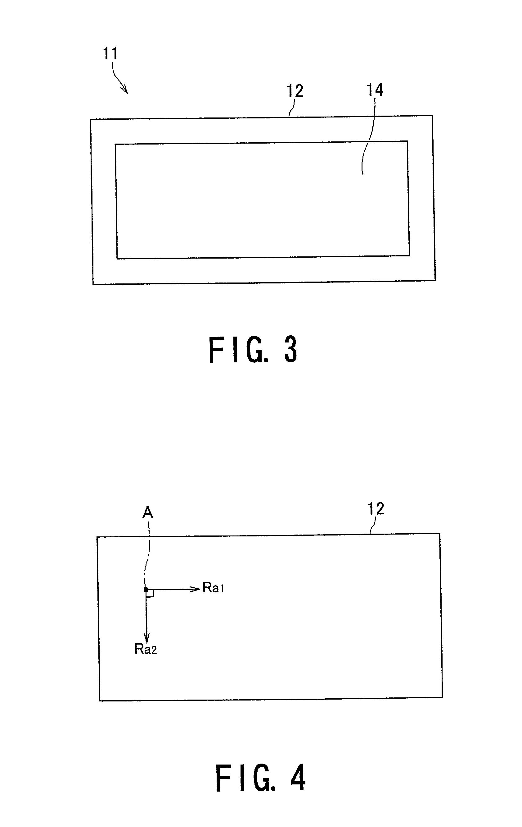
[0127] With respect to silicon nitride sintered bodies each having a thermal conductivity of 90 W / mK and a size of 40 mm.times.60 mm.times.0.32 mm (thickness), a honing treatment and an ultrasonic cleaning treatment as the surface treatments were conducted under the conditions as shown in table 3 thereby to prepare Si.sub.3N.sub.4 substrates for the respective Examples. Note, the grinding work was not performed to the substrates.
[0128] Next, an average value of the ratio Ra1 / Ra2 of the surface roughness Ra in two directions normal to each other of the respective substrates were measured, while the ratio of the chipping flaws formed per unit area of the respective substrates was also measured.
[0129] On the other hand, a brazing material having a composition of 70 Ag-27 Cu-3Ti in terms of mass % was prepared. Then, a copper circuit plate having a thickness of 0.3 mm was bonded to a front surface side of the above Si.sub.3N.sub.4 substrates through the above brazing material, while a r...
PUM
| Property | Measurement | Unit |
|---|---|---|
| thickness | aaaaa | aaaaa |
| thickness | aaaaa | aaaaa |
| surface roughness Ra1 | aaaaa | aaaaa |
Abstract
Description
Claims
Application Information
 - R&D
- Intellectual Property
- Life Sciences
- Materials
- Tech Scout
- Unparalleled Data Quality
- Higher Quality Content
- 60% Fewer Hallucinations
Browse by: Latest US Patents, China's latest patents, Technical Efficacy Thesaurus, Application Domain, Technology Topic, Popular Technical Reports.
© 2025 PatSnap. All rights reserved.Legal|Privacy policy|Modern Slavery Act Transparency Statement|Sitemap|About US| Contact US: help@patsnap.com