

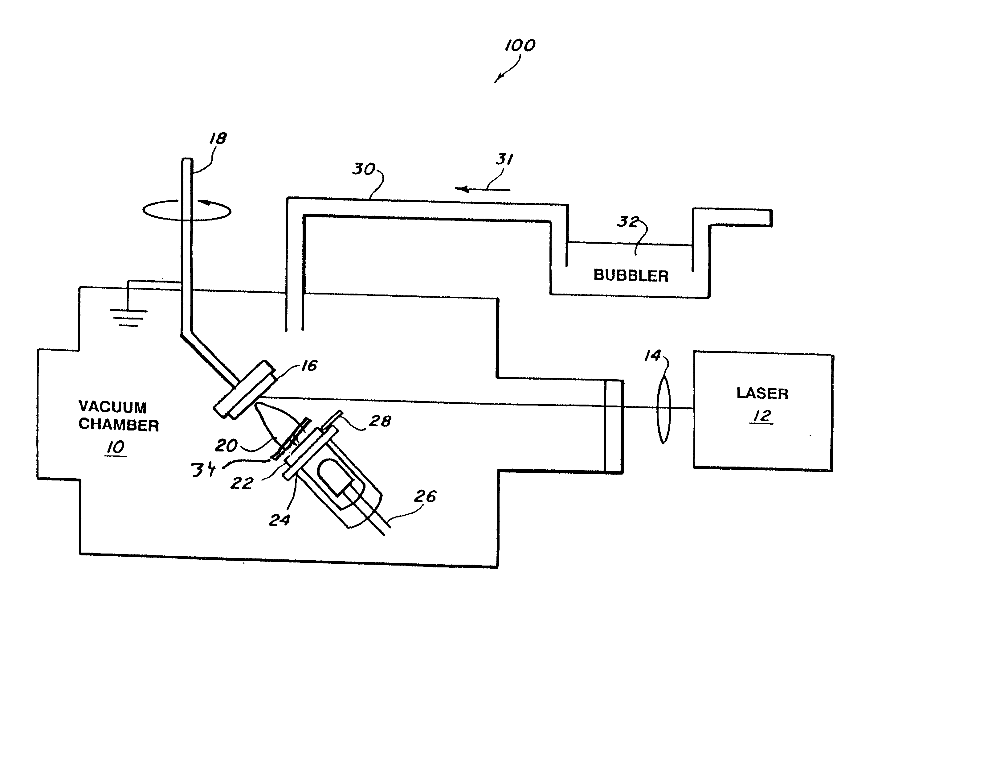
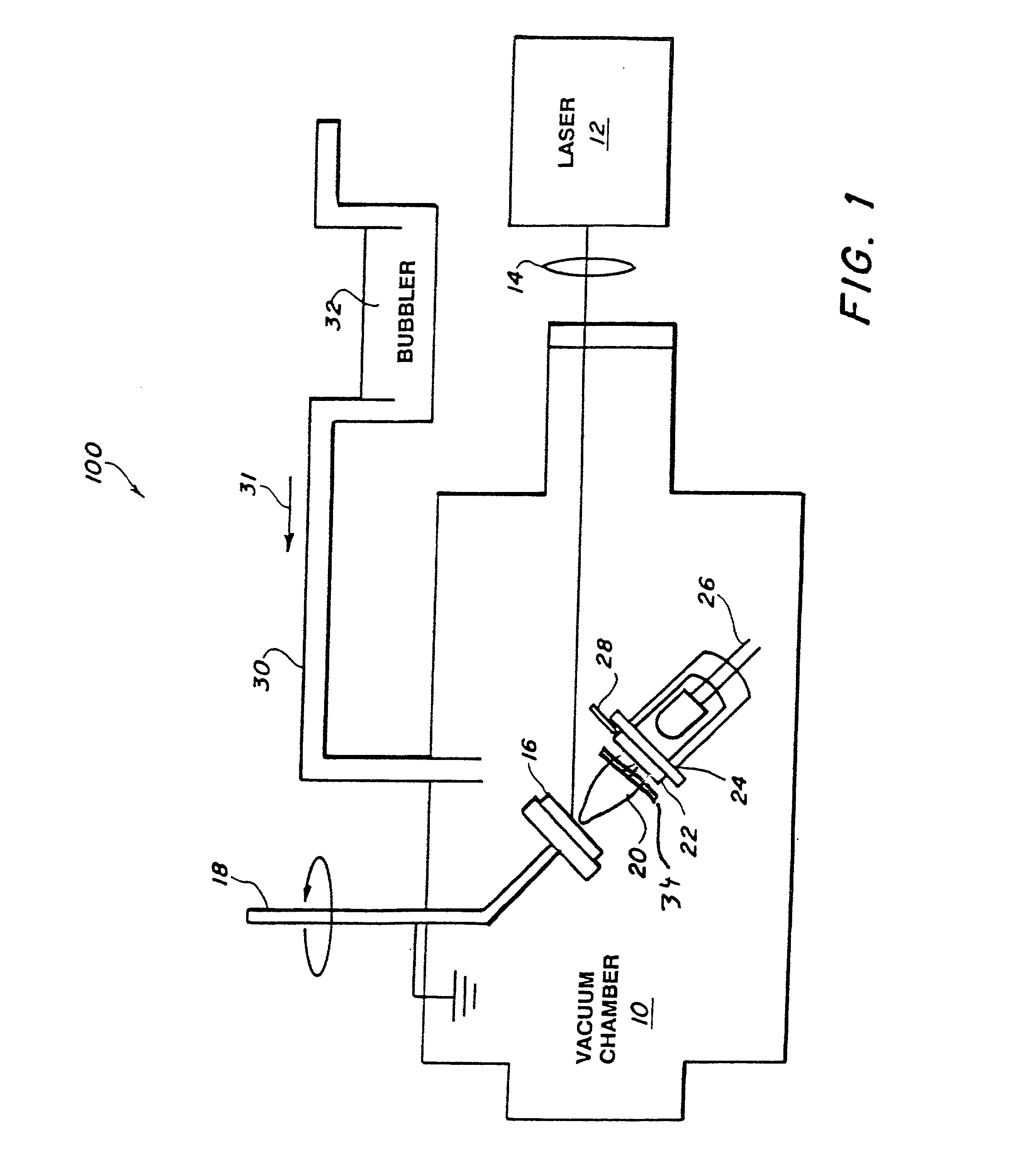
Fabrication of conductive/non-conductive nanocomposites by laser evaporation
a technology of conductive/non-conductive nanocomposites and laser evaporation, which is applied in the field of material deposition, can solve the problems of inability to achieve precise or accurate control of coating thickness with high reproducibility, and the non-uniformity of coatings
- Summary
- Abstract
- Description
- Claims
- Application Information
AI Technical Summary
Problems solved by technology
Method used
Image

Examples
example
[0033] For a polyepichlorohydrin and carbon matrix, a ribbon was prepared by spin coating a film of PECH / graphite on a quartz wafer, at a PECH / graphite thickness of @1 .mu.m from a solution in chloroform. The ribbon was exposed to a pulsed laser that transferred the PECH / graphite matrix to a variety of substrates including glass, ceramics (e.g., alumina), plastics (e.g., polyimide), circuit board composites, silicon and metal surfaces. For demonstration purposes, a 500 nm.times.400 .mu.m.times.250 .mu.m bridge was fabricated over and between two gold electrodes. The gold electrodes had previously been deposited on a printed circuit board. Several test structures were prepared at different resistances. In general, on exposure to an uncalibrated acetone vapor source, the chemiresistors ohmic resistance increased by between 5 and 10% of the initial value 100 K ohm, and in less than 1 second. After removal of the acetone, the resistances returned to their original values in approximatel...
PUM
| Property | Measurement | Unit |
|---|---|---|
| Thickness | aaaaa | aaaaa |
| Thickness | aaaaa | aaaaa |
| Fraction | aaaaa | aaaaa |
Abstract
Description
Claims
Application Information