Passivation of porous semiconductors

a technology of porous semiconductors and semiconductors, applied in the field of porous silicon, can solve the problems of slow degradation of photoluminescence exposure to air, restricting the use of psi in the fabrication of commercial devices, and concomitant degradation of material electronic properties, etc., and achieves unprecedented stability, low defect density, and high chemical stability.

Inactive Publication Date: 2002-09-12
NAT RES COUNCIL OF CANADA
View PDF0 Cites 10 Cited by
  • Summary
  • Abstract
  • Description
  • Claims
  • Application Information

AI Technical Summary

Benefits of technology

[0015] If used without purification it is found that the reactants react at much lower temperatures due to the decomposition of peroxide and hydroperoxide impurities. The inventors have made the unexpected discovery that the non-catalytic thermally-induced hydrosilylation of PSi surfaces with alkenes and aldehydes can result in highly stable structures. Passivated silicon made in accordance with the teachings of the invention has been shown to produce stable electroluminescence for more than 6 hours. The methods in accordance with the invention are believed to be capable of stabilizing blue and green luminescent porous silicon. Generally, the prior art methods have been found to degrade the surface of the silicon so that only red luminescence is possible.

Problems solved by technology

The hydrogen-passivated PSi film is of good electronic quality, but the monolayer of hydrogen formed on its surface does not protect against photoluminescence quenching from chemical adsorbates leading to slow degradation of photoluminescence exposure to air and concomitant degradation of the electronic properties of the material.
This limitation restricts the use of PSi in the fabrication of commercial devices.
However, passivation of the PSi surface by oxidation restricts the photoluminescence to red wavelengths, and is not suitable for stabilizing the photoluminescence of high porosity PSi.
However, the presence of metals such as iron on the semiconductor surface may severely limit the use of PSi in advanced semiconductor technology.
Metals have been found not to provide good coverage within the pores.
Organic molecules have been found to provide the best results, but they still suffer from the fact that eventually oxidation occurs.
Bateman et al, Chem Int. Ed. 1998, 37, 2683-2685 described the application of organic molecules at elevated temperatures, but it is found that structures made by his method are partially oxidized, have poor chemical stability and poor luminescence properties.
Metals have been found not to provide good coverage within the pores.
Organic molecules have been found to provide the best results, but they still suffer from the fact that eventually oxidation occurs.

Method used


Image

  • Passivation of porous semiconductors
  • Passivation of porous semiconductors
  • Passivation of porous semiconductors

Examples


example

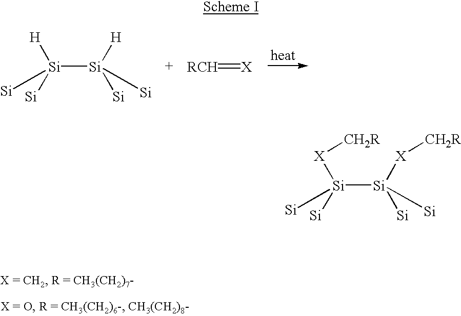
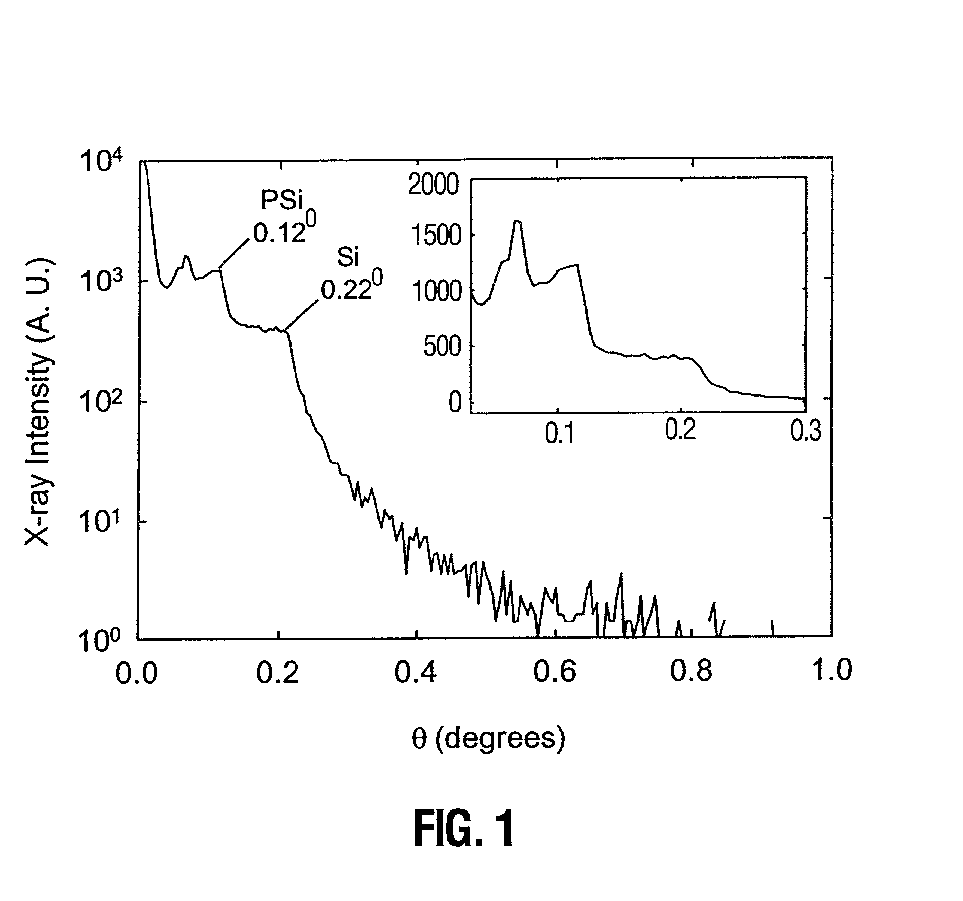
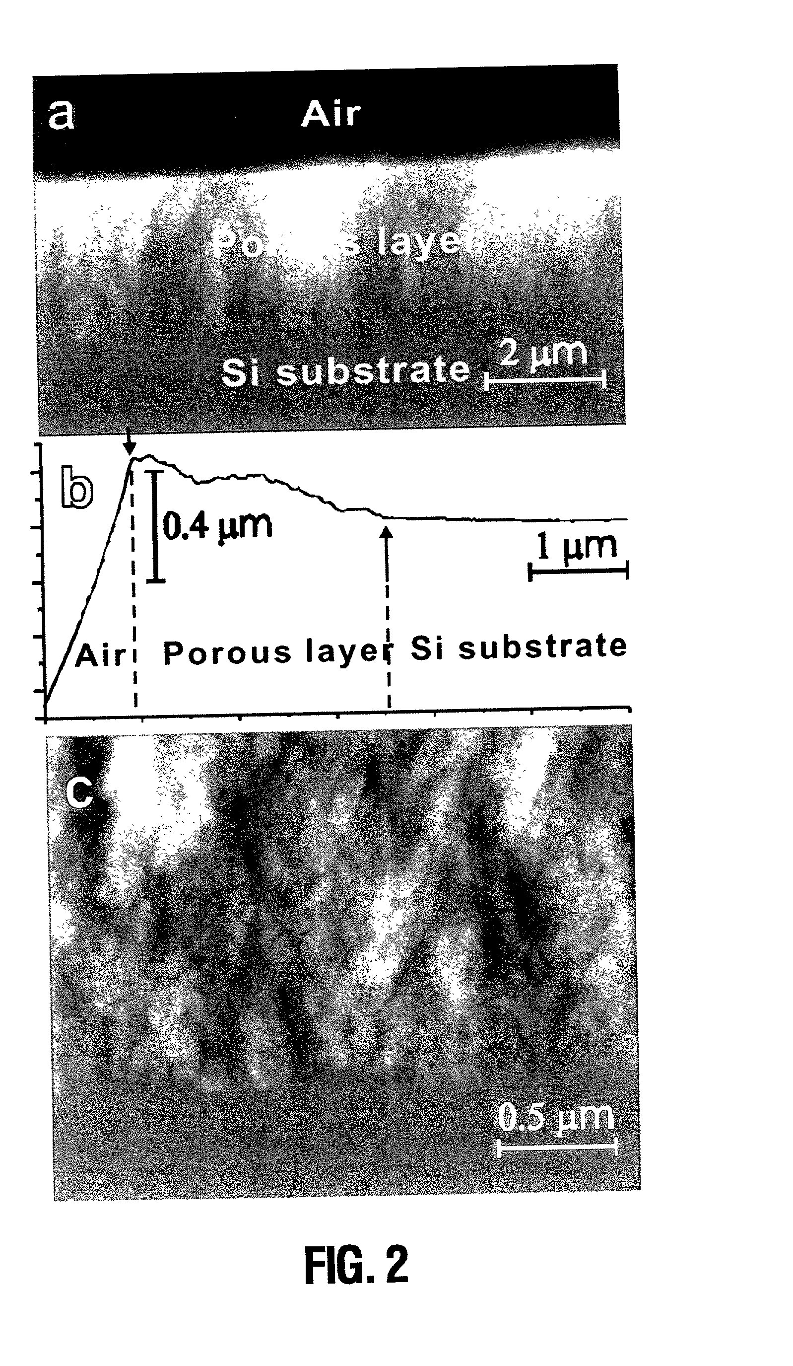
[0031] Silicon wafers were purchased from Virginia semiconductor. All cleaning and etching reagents were clean room grade (Olin Microelectronics Materials). All other reagents were obtained from Aldrich and were the highest purity available. Single side polished (100) oriented p-type silicon wafers (B-doped, 1-1.05 ohm-cm resistivity) were first cleaned in 3:1 concentrated H.sub.2SO.sub.4 / 30% H.sub.2O.sub.2 for 5 min at room temperature and then rinsed copiously with Milli-Q water. The clean wafers were immersed in 48% aqueous HF solution for 1min at room temperature to remove the native-oxide. The hydrogen-terminated surfaces were electrochemically etched in a 1:1 (v / v) pure ethanol and 48% aqueous HF for 8 min at a current density of 5 mA / cm.sup.2. After etching, the samples were rinsed with pure ethanol and dried under a stream of dry nitrogen prior to use. Atomic force microscopy (AFM) in contact mode showed that PSi films prepared in this way are 2.5 to 3 .mu.m thick with an av...


PUM

PropertyMeasurementUnit
temperatureaaaaaaaaaa

Abstract

A method is disclosed for stabilizing porous silicon. A porous silicon structure having a surface terminated with hydrogen atoms is subjected to organic thermal processing to substitute the hydrogen atoms with a protective organic layer. The resulting structure are found to have unprecedented stability.

Description

FIELD OF THE INVENTION[0001] This invention relates to the field of porous semiconductors, and in particular to porous silicon. More particularly, it relates to a method of stabilizing H-terminated porous silicon.BACKGROUND OF THE INVENTION[0002] Since the first report on the efficient visible photoluminescence of porous silicon (PSi) under (ultra violet) UV excitation, at room temperature, this material has generated world wide interest. There has been a vast amount of work devoted to the structural, optical and electronic aspects of this material in order to understand the origins of the photoluminescence and to develop applications in solid-state electroluminescent devices. Because of its tunable electroluminescent and photoluminescent properties, applications in silicon-based optoelectronics, which have hitherto been severely constrained by the weak luminescence of indirect band-gap bulk silicon, have become feasible. The origin of the quantum confined photoluminescence is belie...

Claims


Application Information

Patent Timeline
Patent Type & Authority Applications(United States)
IPC IPC(8): B05D1/18B05D7/24H01L21/306
CPCB05D1/185B05D1/60B82Y30/00B82Y40/00H01L21/306Y10S436/805Y10S436/823
Inventor BOUKHERROUB, RABAHWAYNER, DANIAL D.M.LOCKWOOD, DAVID J.MORIN, SYLVIE
Owner NAT RES COUNCIL OF CANADA
Why Eureka
Try Eureka