Method for manufacturing a semiconductor device

a semiconductor and manufacturing technology, applied in the direction of transistors, electric devices, basic electric elements, etc., can solve the problem of difficult formation of diffusion layers thinner than the above-indicated lower limit, and achieve the effect of high yield

a semiconductor and manufacturing technology, applied in the direction of transistors, electric devices, basic electric elements, etc., can solve the problem of difficult formation of diffusion layers thinner than the above-indicated lower limit, and achieve the effect of high yield

US20020127783A1Inactive Publication Date: 2002-09-12FUJI ELECTRIC CO LTD

Image

  • Method for manufacturing a semiconductor device
  • Method for manufacturing a semiconductor device
  • Method for manufacturing a semiconductor device

Examples


Embodiment Construction

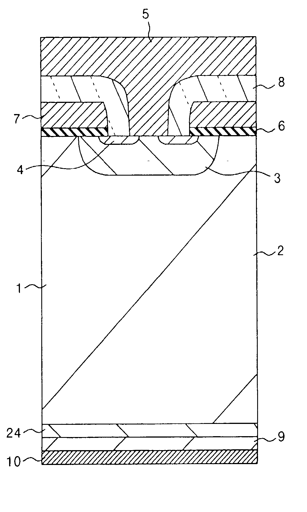
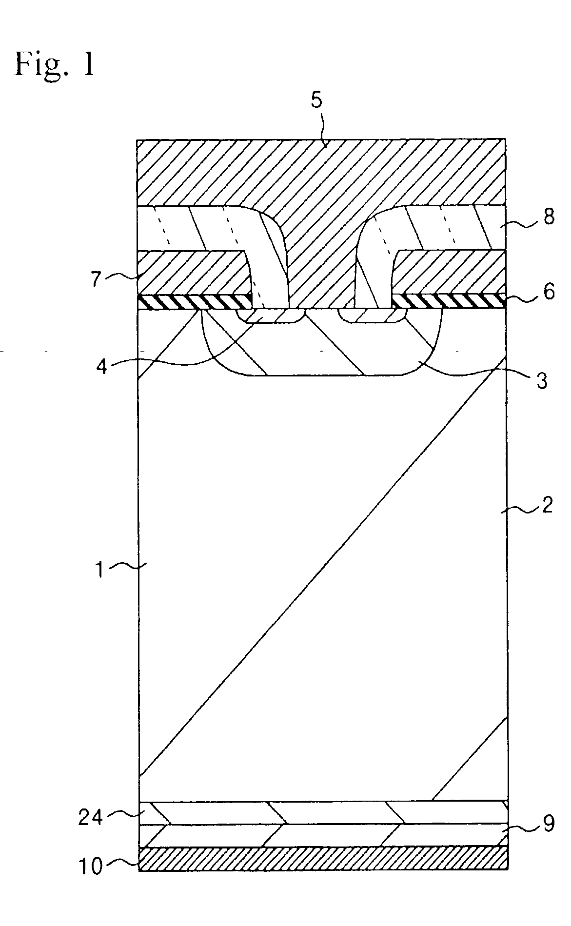
[0053] FIG. 1 is a cross-sectional view of an example of a semiconductor device manufactured by a method according to the present invention. The illustrated semiconductor device is an IGBT with a planar gate structure including a base layer 2 that is composed, for example, of an n-type semiconductor substrate 1 made of a silicon FZ wafer. On the surface region of the base layer 2, a p-type channel diffusion region 3 is formed. In this channel diffusion region 3, an n-type emitter diffusion region 4 is formed.

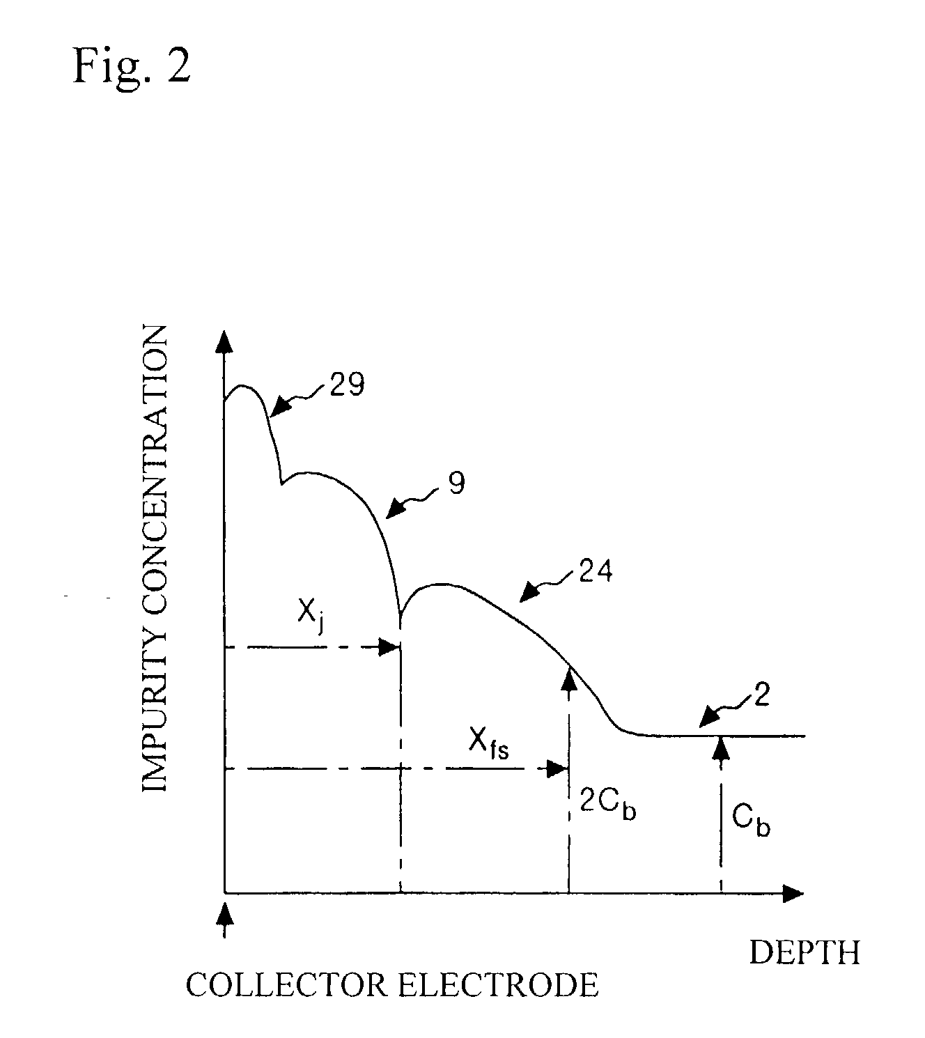
[0054] On a part of this emitter diffusion region 4, a gate electrode 7 is formed through a gate-insulating film 6. An emitter electrode 5 is electrically connected to the channel diffusion layer 3 and the emitter diffusion region 4, and insulated from the gate electrode 7 through an insulator film 8. In a shallow portion of the reverse surface region of the base layer 2, a field-stop layer 24 composed of an n-type impurity diffusion layer is formed. A p-type collector layer 9 i...


PUM


Abstract

A method for manufacturing a semiconductor device constituting an IGBT is provided that allows to manufacture the device using an inexpensive wafer and with high yields, and achieves low losses. Specifically, after an emitter electrode is formed, a reverse principal surface is polished to a specified thickness. The center line average height Ra of the polished surface is controlled to be not more than 1 .mu.m, and the filtered center line waviness Wca is kept within 10 .mu.m. The polished surface is selectively cleaned with chemicals-dissolved water to remove particles. To the cleaned surface, phosphorus ions are implanted for forming a field-stop layer and boron ions are implanted for forming a collector layer. The wafer is then put into a diffusion furnace and annealed at a temperature from 300.degree. C. to 550.degree. C. to form a field-stop layer and a collector layer. Finally, a collector electrode is formed.

Description

FIELD OF THE INVENTION[0001] The present invention relates to a method for manufacturing a semiconductor device and in particular, to a method for manufacturing a semiconductor device that constitutes an insulated gate bipolar transistor.BACKGROUND[0002] Insulated gate bipolar transistors (hereinafter referred to as IGBTS), specifically the devices of planar gate structures as shown in FIG. 30 and FIG. 31 and the devices of trench gate structures as shown in FIG. 32 and FIG. 33, are known. A non-punch-through type IGBT as shown in FIG. 30 or FIG. 32 comprises a base layer 2 that is composed of an n-type semiconductor substrate made of for example an FZ wafer; a p-type channel diffusion region 3, an n-type emitter diffusion region 4, an emitter electrode 5, a gate-insulating film 6, a gate electrode 7, and an insulator film 8, which are formed on one surface of the substrate; and a p-type collector layer 9 and a collector electrode 10, which are formed on the reverse surface side of ...

Claims


Application Information

Patent Timeline
12 Sep 2002
Publication
US20020127783A1
IPC
H01L21/331
CPC
H01L29/66333
Inventors
OTSUKI, MASAHITO; MOMOTA, SEIJI