Multi-band power amplifier

a multi-band, power amplifier technology, applied in the field of amplifiers, can solve the problems of increasing the loss of collectors to generate heat, destroying the final-stage power amplification transistor, and reducing the current concentration due to generated hea

Inactive Publication Date: 2003-06-26
RENESAS ELECTRONICS CORP
View PDF4 Cites 21 Cited by
  • Summary
  • Abstract
  • Description
  • Claims
  • Application Information

AI Technical Summary

Benefits of technology

[0075] In particular, even when the first and second unit transistor cells are mixedly formed in a transistor cell formation region and the effective pitches of the unit transistor cells are reduced to reduce a thermal resistance, a noise component generated through capacitive coupling of a harmonic component can also be prevented. A chip size can be efficiently reduced without impairing transmission quality and destruction of the element due to current concentration can be prevented.
[0076] Furthermore, by arranging the unit transistor cells to surround each other, the unit cells in operation are free of thermal boundary and in the transistor region in operation, heat is dissipated to suppress heat concentration and hence prevent current concentration from occurring.
[0077] Furthermore, when the first and second output transistors have their unit transistor cells arranged alternately, unit transistor cells that simultaneously operate can be arranged in a dispersed manner in the transistor formation region. Accordingly, thermal resistance can be reduced, heat generation can be suppressed, and the unit transistor cells can also have a reduced pitch, and accordingly, a reduced chip size can be achieved.

Problems solved by technology

When an output load varies under the high power supply voltage condition, collector loss is increased to generate heat due to the current loss in the collector loss, and transistor cells constructing a power amplification transistor operate ununiformly.
In particular, the ununiform operation of unit cell transistors in final-stage power amplification transistor Trg3 or Trd3 would cause a current concentration that the operating currents of a part of unit cell transistors occupy a major portion of the whole operating current of the final-stage transistor.
Consequently, variation in power output within a pulse in a burst operation is introduced and in the worst case, the final-stage power amplification transistor would be eventually destroyed.
Such current concentration due to generated heat is a disadvantage peculiar to a power amplifier having a plurality of unit transistor cells arranged closely adjacent to each other within a chip.
This, however, increases the layout area of the final-stage power amplification transistor and the increased area of the final-stage power amplification transistor, which occupies a large area of the chip, increases the chip size.
In particular, in a case of an HBT amplifier formed of a compound semiconductor such as GaAs, it is more expensive than a Si-MOSFET and reduction of chip area is important in view of price.
Furthermore, if the unit transistors of DCS and GSM output transistors are arranged in separate regions with a sufficient pitch condition in each region, and the separate regions for GSM and for DCS, similarly, due to a capacitive coupling between interconnection lines, a noise is superimposed and transmission quality is impaired.
Furthermore, in this case, in view of reduction of chip area, the pitch of the unit transistors cannot sufficiently be increased, and the issue of the current concentration cannot sufficiently be overcome.

Method used


Image

  • Multi-band power amplifier
  • Multi-band power amplifier
  • Multi-band power amplifier

Examples


first embodiment

[0099] First Embodiment

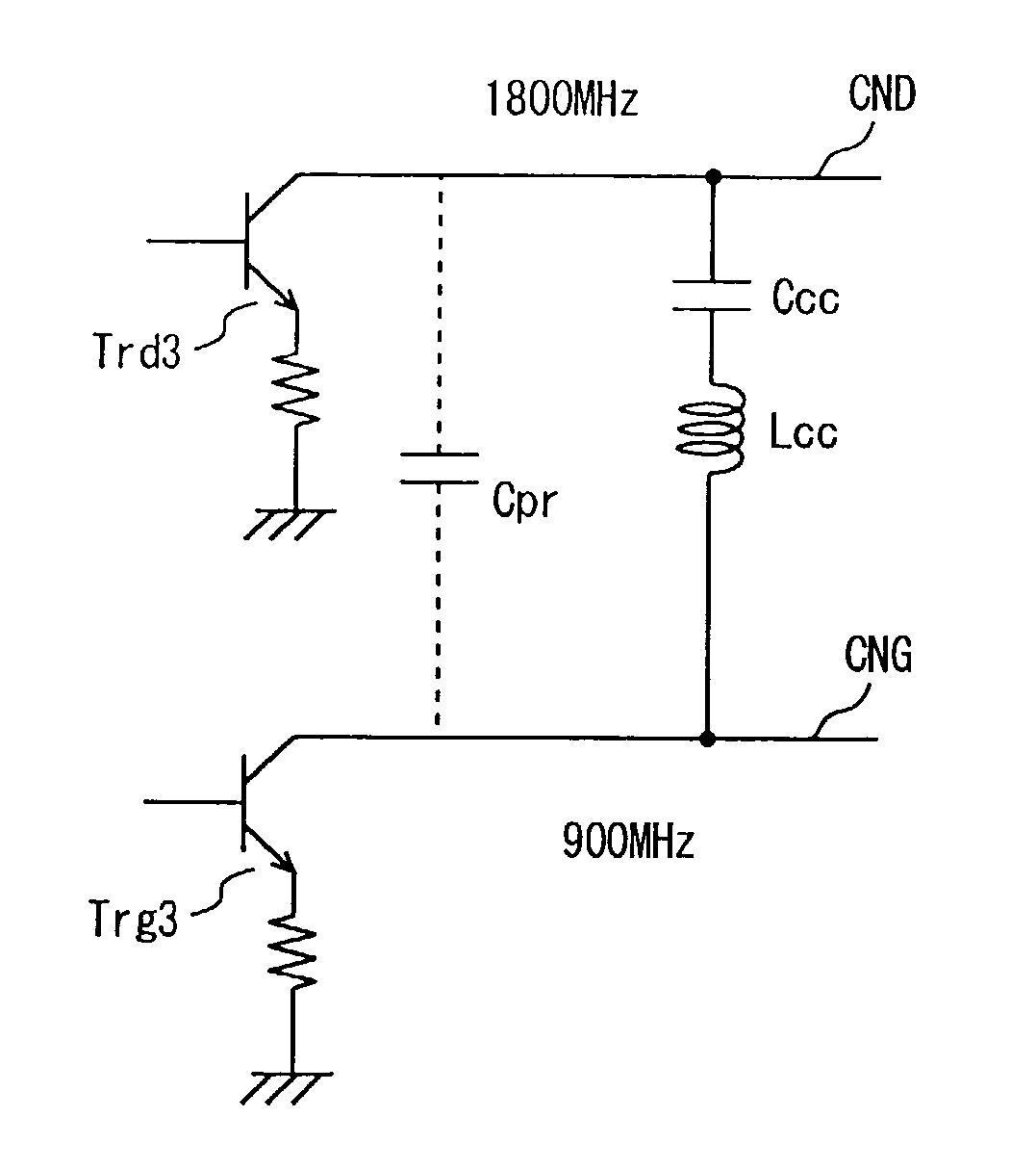
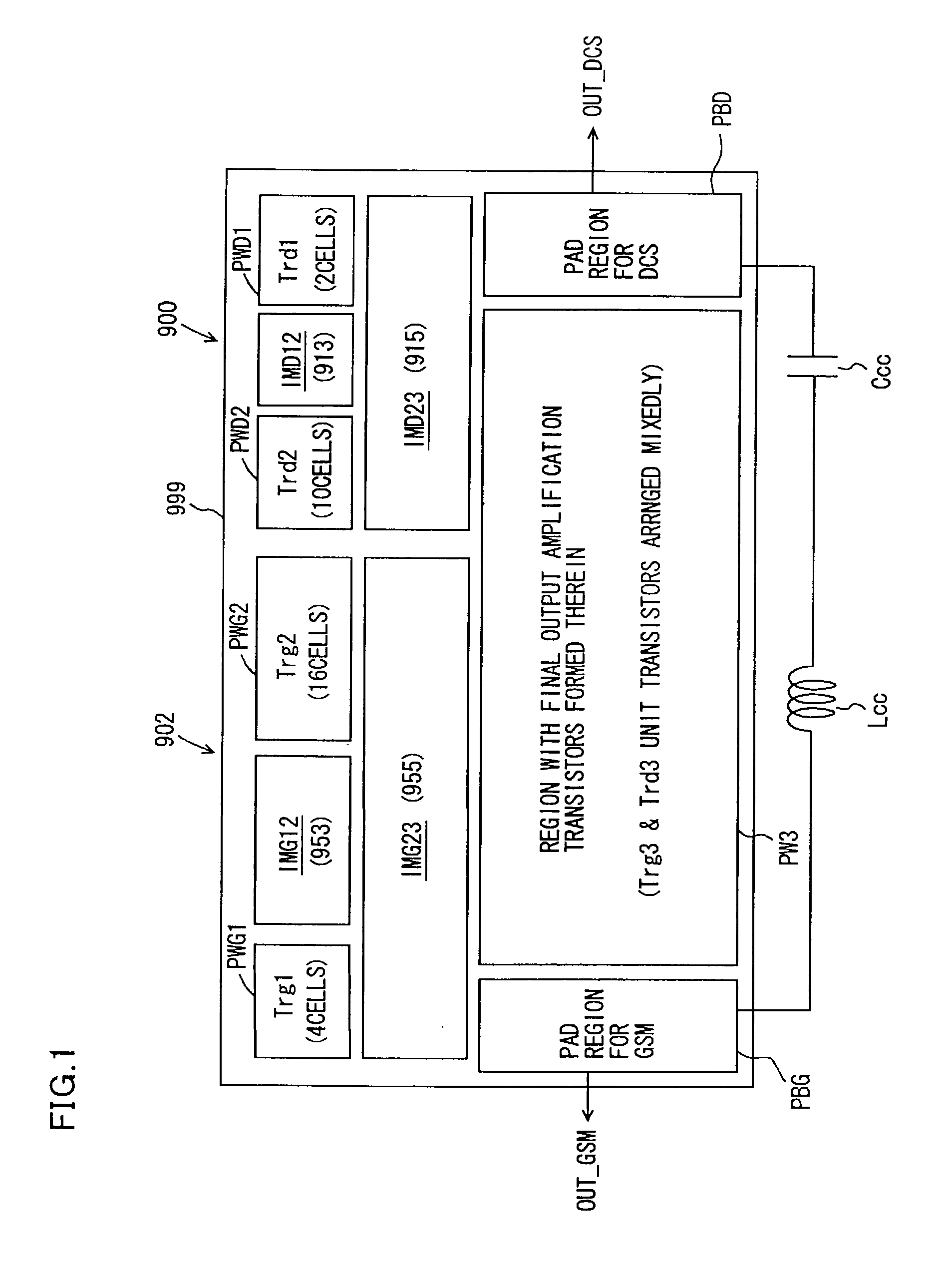
[0100] FIG. 1 schematically shows a layout of a chip of a DCS / GSM dual-band power amplification circuit in accordance with a first embodiment of the present invention. The dual-band power amplification circuit of FIG. 1 is different in layout from that shown in FIG. 18 in the following points. Unit transistors (Tr) for constructing final-stage output power amplification transistors Trd3 and Trg3 of the respective DCS and GSM power amplifiers are arranged in a mixed manner in a region PW3 for forming the final output amplification transistors.

[0101] A DCS pad region PBD and a GSM pad region PBG are arranged opposite each other with respect to the region PW3. The DCS final-stage power amplification transistor has its collector connected to an output line connected to pads in DCS pad region PBD to output an output signal OUT_DCS.

[0102] The GSM final-stage power amplification transistor has its collector connected to an output line connected to pads included in DS...

second embodiment

[0115] Second Embodiment

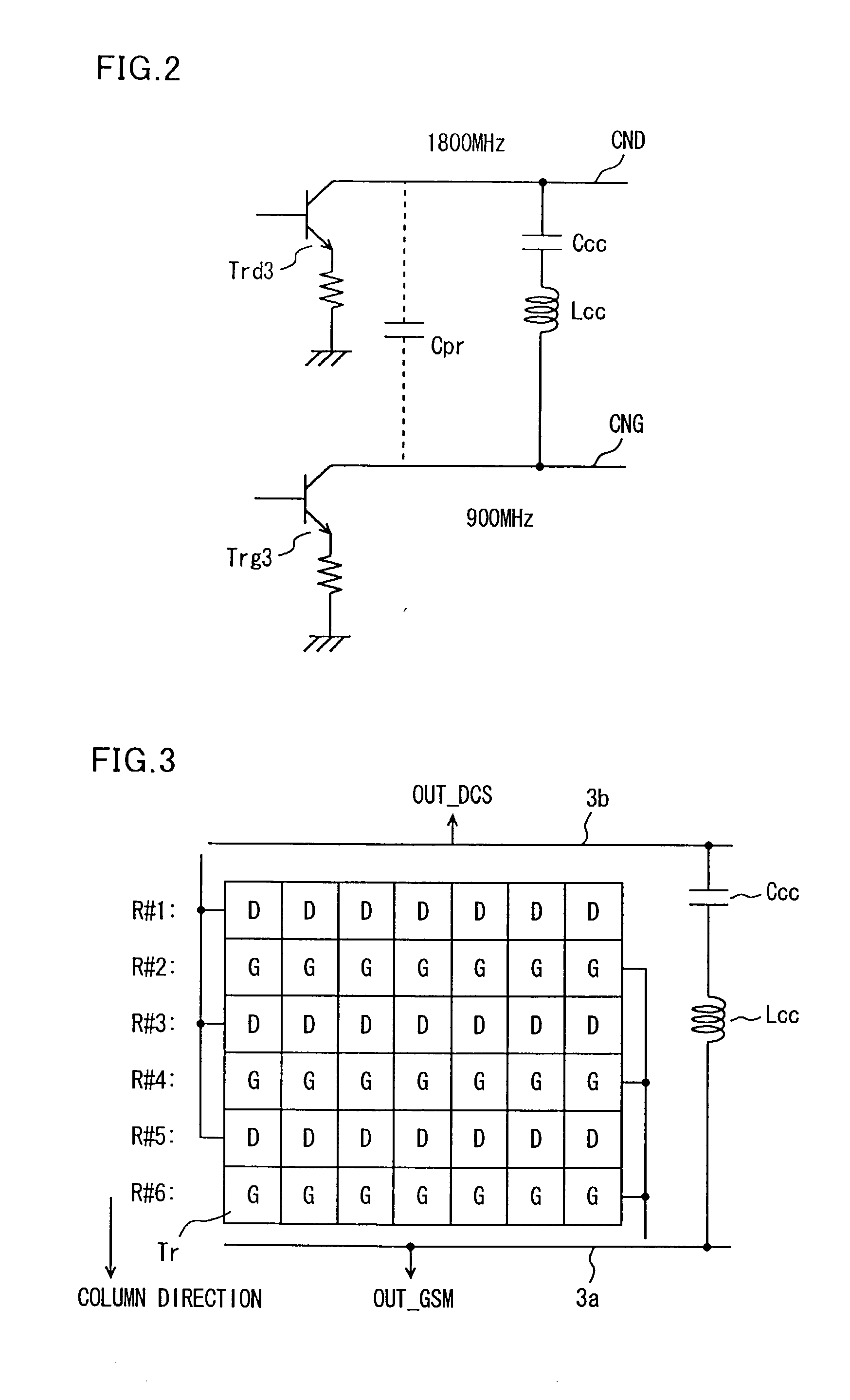
[0116] FIG. 3 schematically shows an arrangement of unit transistor Tr of the final-stage power amplification transistor in accordance with a second embodiment of the present invention. In FIG. 3, unit transistors Trs are arranged in a plurality of rows and a plurality of columns. FIG. 3 exemplarily shows a layout of arranging unit transistors Trs in six rows and seven columns.

[0117] In this transistor array, unit transistors Trs arranged in odd-numbered rows R#1, R#3 and R#5 are used as the final-stage power amplification transistor of the DCS power amplifier, and unit transistors Trs arranged in even-numbered rows R#2, R#4 and R#6 are used as components of the final-stage power amplification transistor of the GSM power amplifier. In FIG. 3, a letter "D" denotes unit transistor Tr used as a component of the DCS power amplification transistor and a letter "G" denotes unit transistor Tr used as a component of the final-stage power amplification transistor of t...

third embodiment

[0139] Third Embodiment

[0140] FIG. 5 schematically shows an arrangement of unit transistors in accordance with a third embodiment of the present invention. In FIG. 5, unit transistors are arranged in rows and columns. In each of unit transistor rows R#1-R#6, a unit transistor D configuring a DCS power amplification transistor and a unit transistor G configuring a GSM power amplification transistor are arranged alternately. Furthermore, in each of unit transistor columns C#1-C#7, DCS and GSM unit transistors D and G are arranged alternately. That is, in the arrangement of FIG. 5 of unit transistor cells, DCS and GSM unit transistors D and G are arranged alternately, in both of the row direction and the column direction.

[0141] For interconnecting the collectors of GSM unit transistors Gs, sub collector interconnection lines 4a1-4a7 are arranged, in unit transistor columns C#1-C#7, extending in the column direction. For interconnecting the collectors of DCS unit transistors Ds, sub col...


PUM


Abstract

A final-stage power amplification transistor is formed of unit transistors arranged in a mixed manner in a region in which the final output amplification transistors for a multi-band power amplifier is formed. Furthermore, an inductance element is connected between output signal lines to which the final output stage transistors are coupled. Thus, the final-stage transistors in a dual band power amplifier can be made free from current concentration due to heat generation without impairing inter-band isolation.

Description

[0001] 1. Field of the Invention[0002] The present invention relates generally to amplifiers and particularly to configurations of power amplifiers for multi-bands, such as dual bands or triple bands. More specifically, the present invention relates to configurations for preventing degradation of transistor characteristics of a multi-band power amplifier without deterioration of communication quality or increase in chip size.[0003] 2. Description of the Background Art[0004] For power amplifiers for mobile communications, there are currently, commonly used a MMIC (monolithic microwave IC) or module (hybrid IC or multi-chip module) using a GaAs MESFET (metal-semiconductor filed effect transistor), a GaAs HEMT (high electron mobility transistor), or a GaAs HBT (hetero junction bipolar transistor). Of these transistors, a GaAs-HBT or a SiGe-HBT utilizing a hetero junction of gallium arsenide (GaAs) or of silicon germanium (SiGe) is currently most promising power devices for mobile commu...

Claims


Application Information

Patent Timeline
Patent Type & Authority Applications(United States)
IPC IPC(8): H01L21/331H01L21/8222H01L27/06H01L29/73H03F1/30H03F1/52H03F3/21H03F3/213H03F3/60H03F3/72
CPCH03F1/302H03F3/211H03F3/602H03F2203/7209H03F2200/111H03F2200/429H03F3/72
Inventor YAMAMOTO, KAZUYASUZUKI, SATOSHI
Owner RENESAS ELECTRONICS CORP
Why Eureka
Try Eureka