Microdischarge devices and arrays having tapered microcavities

Inactive Publication Date: 2003-07-17
BOARD OF TRUSTEES OF THE UNIV OF ILLINOS
View PDF22 Cites 53 Cited by
  • Summary
  • Abstract
  • Description
  • Claims
  • Application Information

AI Technical Summary

Benefits of technology

0068] Such designs minimize ohmic losses in the electrodes as arrays increase in size and improve the characteristics and reproducibility for igniting the array or collection. In addition, these designs decrease the voltage variation appearing across individual devices in at least 10 of the devices in the array. This decrease is such that when a minimum voltage sufficient to cause discharging of at least 10 of the devices is applied then the voltage difference between the first and second electrodes at every cavity of the microdischarge devices has a voltage difference of no more than 20% of the average voltage difference. The lower the voltage difference

Problems solved by technology

Most of these devices are, unfortunately, bulky and frequently have fragile quartz or glass envelopes and require expensive mounting fixtures.
Despite their applications in several areas, including optoelectronics and sensors, microdischarge devices can have several drawbacks.
For example, the lifetime of the devices is exceedingly short, operating for only a few tens of hours.
Damage to the anode is quickly visible and is caused by sputtering.
Extracting optical power from deep cylindrical cavities is also frequently ineffic

Method used


Image

  • Microdischarge devices and arrays having tapered microcavities
  • Microdischarge devices and arrays having tapered microcavities
  • Microdischarge devices and arrays having tapered microcavities

Examples


Embodiment Construction

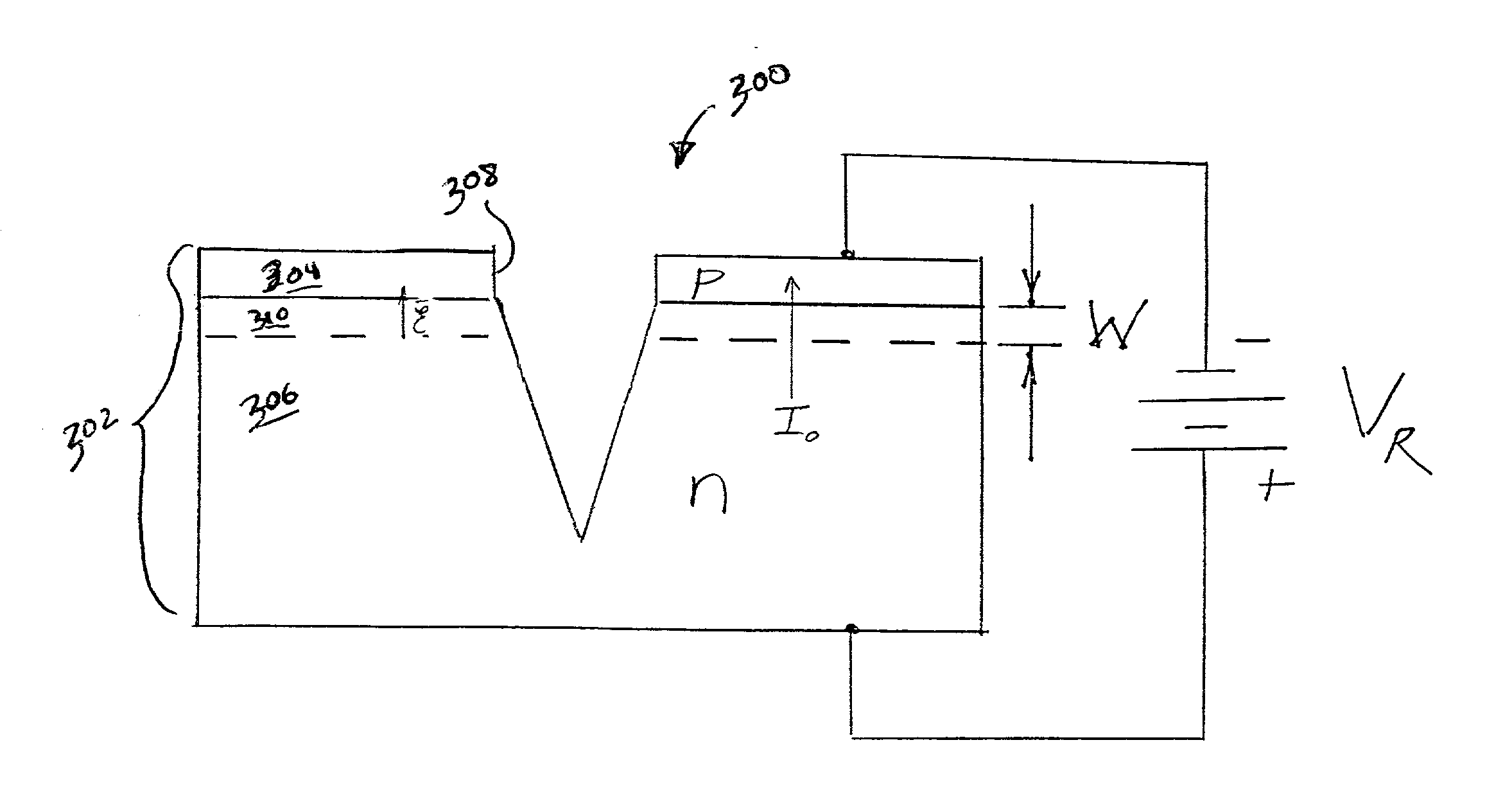
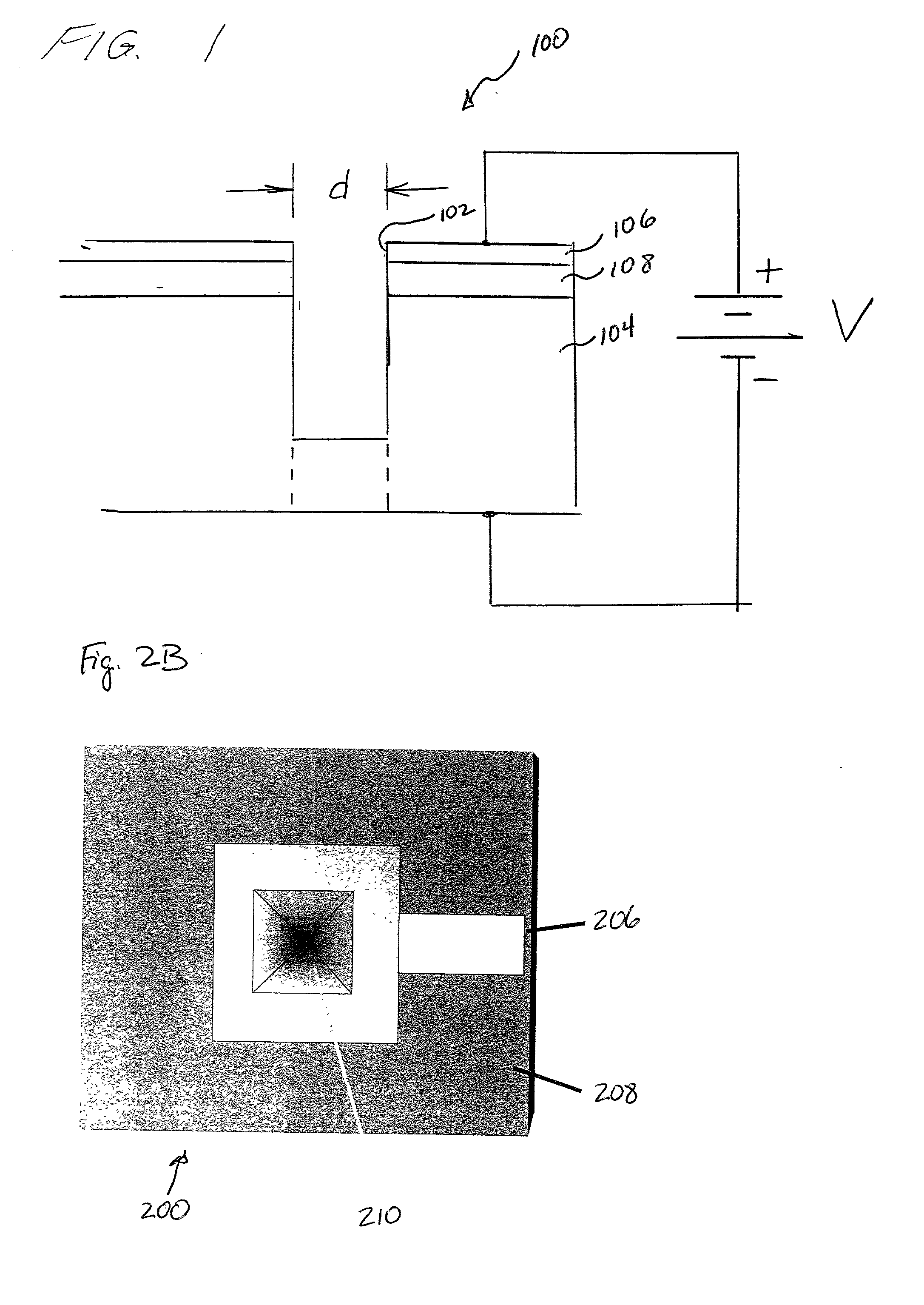
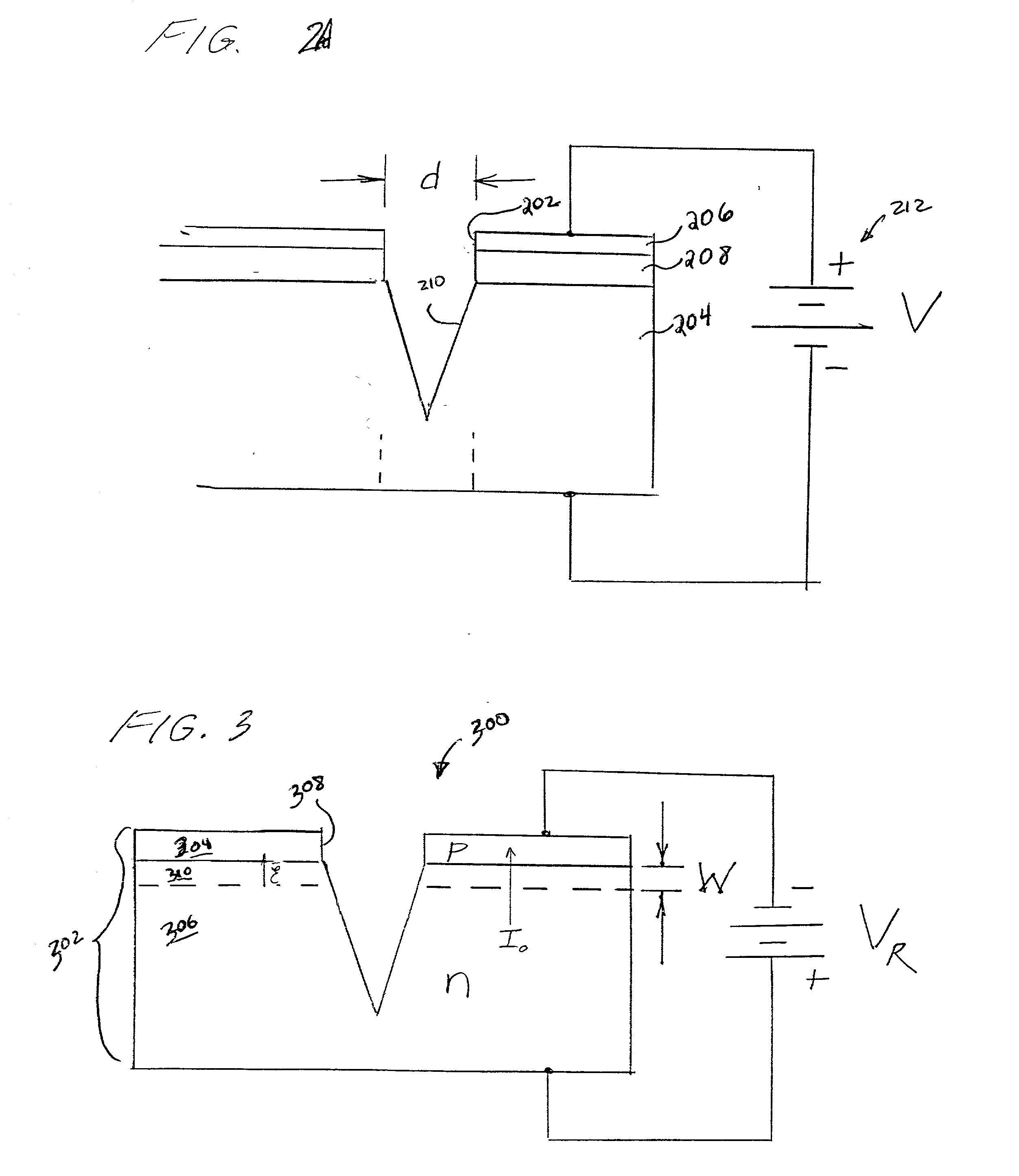
[0070] Devices were fabricated in p-type silicon (100) wafers having a resistivity of 6-8 .OMEGA.-cm and a typical thickness of 300 .mu.m. Pyramidal cavities, 50 or 100 .mu.m square at the base and of 35 .mu.m or 70 .mu.m depth, respectively, were fabricated. The cavities were produced by anisotropic wet etching in a 33% (wt / wt) solution of KOH in water. Subsequently, the device dielectric was formed by spin coating an approximately 7.5-8 .mu.m thick layer of a dry etchable polyimide (Dupont 2611, relative permittivity .epsilon..sub.r=2.9) onto the silicon surface followed by curing the polymer at 300.degree. C. in a N.sub.2 atmosphere. Subsequently, a 1200-2400 .ANG. thick Ni film was e-beam evaporated onto the polyimide to serve as the anode. The discharge channels in the metal anode and dielectric films were defined photolithographically with a Cr mask and etched by wet and reactive ion etched (O.sub.2 plasma) processes, respectively. Some devices additionally had SiO.sub.2 or Si...


PUM


Abstract

A microdischarge device has a semiconductor layer, an intermediate layer, and a conductive layer. A tapered cavity is disposed in at least the semiconductor layer.

Description

[0001] The present invention relates to microdischarge devices and, in particular, to novel structures for light emitting devices. It has long been known that electrical discharges are efficient sources of light, and today gas discharge lamps (including fluorescent sources, and metal-halide, sodium, or mercury arc lamps) account for most of the world's light-generating capacity (several billion watts on a continuous basis). Most of these devices are, unfortunately, bulky and frequently have fragile quartz or glass envelopes and require expensive mounting fixtures. In addition to general lighting, discharges produce ultraviolet and visible light for other purposes, such as germicidal applications (disinfecting surfaces and tissue), cleaning electronic and optical surfaces in manufacturing, curing polymers and activating light-sensitive molecules for medical treatments and diagnostics.[0002] Although discharge devices were apparently first demonstrated by A. D. White in 1959, only rec...

Claims


Application Information

Patent Timeline
IPC IPC(8): H01J11/18H01J17/06H01J17/10H01J17/49H01J61/09H01J61/62
CPCH01J11/18H01J17/066H01J61/62H01J17/49H01J61/09H01J17/10
Inventor EDEN, J. GARYPARK, SUNG-JINCHEN, JACKLIU, CHANG
Owner BOARD OF TRUSTEES OF THE UNIV OF ILLINOS
Why Eureka
Try Eureka