
Resist material and method for forming a resist pattern with the resist material

Inactive Publication Date: 2003-07-31
FUJITSU SEMICON LTD
View PDF0 Cites 36 Cited by
  • Summary
  • Abstract
  • Description
  • Claims
  • Application Information

AI Technical Summary

Benefits of technology

[0017] Accordingly, in cases where the resist material according to the present invention is used according to the above resist pattern forming method, the thin film can be correctly patterned even though a minimum pattern width required for the thin film is moreover shortened. Therefore, the resist material and the resist pattern forming method are useful for the manufacturing a semiconductor apparatus such as a semiconductor integrated circuit or the like.

Problems solved by technology

However, there is a case that a type of layer planned to be etched moreover requires of the dry-etching resistance.
However, it is difficult to heighten the dry-etching resistance in cases where the above conventional resist having a structure of the acrylate resin is used.

Method used


Image

  • Resist material and method for forming a resist pattern with the resist material
  • Resist material and method for forming a resist pattern with the resist material
  • Resist material and method for forming a resist pattern with the resist material

Examples


second example

[0088] The second example differs from the first example in that another developer is used and a threshold energy Eth of quantity of radiation is 25.6 mJ / cm.sup.2. That is, a pattern resist film is formed according to the same method as in the first example.

[0089] As the developer, a solution of the tetrabutyl ammonium hydroxide (TBAH) having a concentration of 0.27 N is used.

[0090] As a result, a pattern resist film is obtained in the same manner as in the first example. Because of the threshold energy Eth of 25.6 mJ / cm.sub.2, a resolving power of 0.275 .mu.m at line and space is obtained.

third example

[0091] The third example differs from the first example in that another developer is used and a threshold energy Eth of quantity of radiation is 9.6 mJ / cm.sup.2. That is, a pattern resist film is formed according to the same method as in the first example.

[0092] As the developer, a solution obtained by mixing the TMAH solution of 0.27 N with iso-propyl-alcohol (IPA) is used. A mixing ratio is 3 (TMAH) to 1 (IPA).

[0093] As a result, a pattern resist film is obtained in the same manner as in the first example. Because of the threshold energy Eth of 9.6 mJ / cm.sup.2, a resolving power of 0.325 .mu.m at line and space is obtained.

fourth example

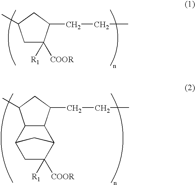
[0094] The triphenylsulfonium hexafluoroantimonate is added to cyclic hydrocarbon resin expressed by a chemical structural formula (34) as the acid generating agent to form a mixed product in which the triphenylsulfonium hexafluoroantimonate is included by 5% by weight, the mixed product is dissolved in the cyclo-hexane, and a resist solution is obtained. 18

[0095] Thereafter, the resist solution is spin-coated on a silicon substrate at a film thickness of 0.7 .mu.m. In this case, a surface of the silicon substrate is cleaned in advance with the HMDS. Thereafter, the silicon substrate is pre-baked on a hot plate for 100 seconds at a temperature of 100.degree. C. to form a resist film. Thereafter, the resist film is selectively irradiated with KrF laser having a wavelength of 248 nm by using the KrF excimer stepper (NA=0.45) manufactured by the Nikon corporation, and a latent pattern is formed in the resist film.

[0096] Thereafter, the resist film in which the latent pattern is formed ...


PUM


Abstract

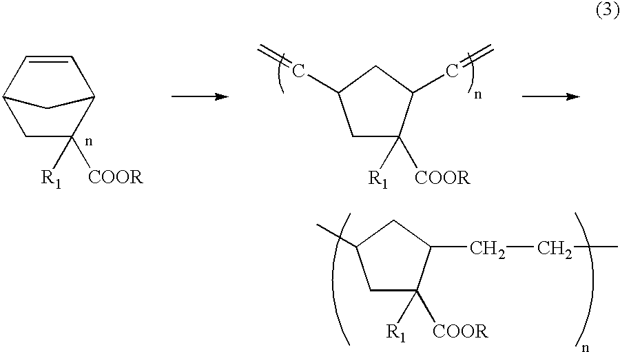
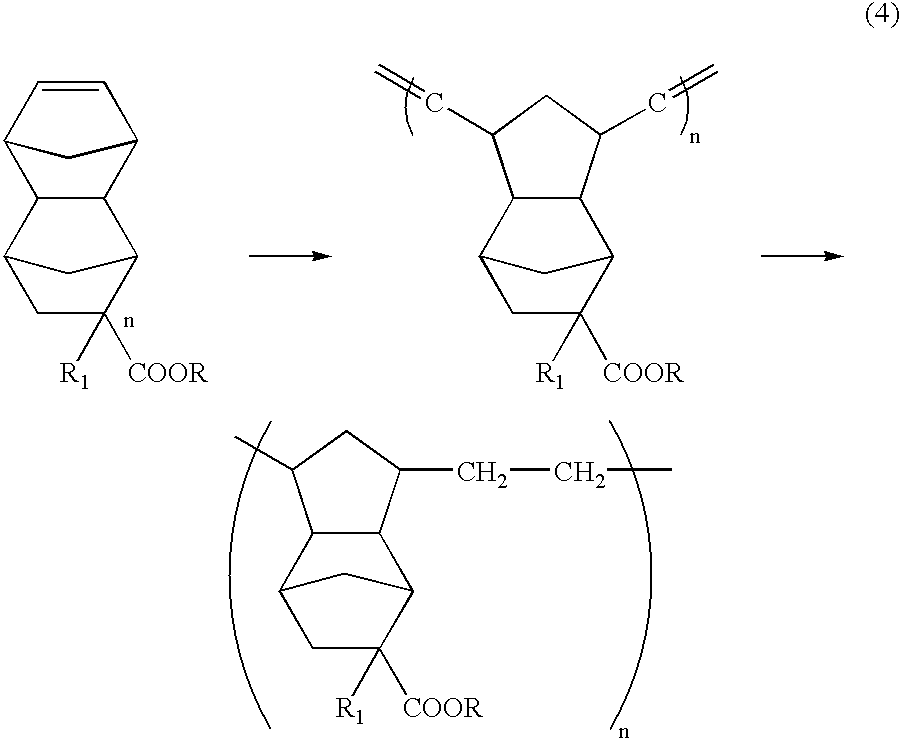
A resist material is made of a polymer or copolymer having a cyclic hydrocarbon as a skeletal structure and an alkali-soluble group to which a protective group is attached as a side chain. Because of the protective group, the resist material is insoluble in alkali solution. In addition, an acid generating agent is added to the resist material. When the acid generating agent is irradiated with a radiation ray, an acid is generated from the acid generating agent, and the protective group is detached from the alkali-soluble group by the function of the acid. Therefore, a resist film made of the resist material can be formed in a desired pattern by irradiating the resist film with the radiation ray. Also, because the cyclic hydrocarbon is used as the skeletal structure of the polymer or copolymer, a superior dry-etching resistance is obtained as compared with a conventional resist material in which acrylate resin is used as a skeletal structure, so that there is no probability that a patterned resist film is over-etched or deformed even though the patterned resist film is used as a mask in an etching process.

Description

[0001] 1. Field of the Invention[0002] The present invention relates generally to a resist material and a method for forming a resist pattern with the resist material, and more particularly to a chemical amplifier resist and a method for forming a resist pattern with the chemical amplifier resist material.[0003] 2. Description of the Prior Art[0004] An integration degree in a semiconductor integrated circuit has been heightened, a large scale integrated circuit (LSI) and a very large scale integrated circuit (VLSI) are put to practical use, a minimum pattern width in the integrated circuit is on the order of sub-microns, and the minimum pattern width has been moreover shortened.[0005] When a micro-pattern is formed, a thin film or a substrate planned to be patterned is covered with a resist, the resist is selectively exposed to light to form a latent image of a desired pattern in the resist, the resist is developed, and a patterned resist is formed on the thin film or the substrate....

Claims


Application Information

Patent Timeline
IPC IPC(8): G03F7/039G03F7/004G03F7/32G03F7/38H01L21/027
CPCG03F7/0045Y10S430/106G03F7/322G03F7/0395
Inventor TAKECHI, SATOSHI
Owner FUJITSU SEMICON LTD
Learn More