High throughput process for the formation of a refractory metal nucleation layer

a refractory metal and nucleation layer technology, applied in the direction of basic electric elements, semiconductor devices, electrical equipment, etc., can solve the problems of long "incubation time, difficult to initiate, poor thickness uniformity of tungsten layers,

Inactive Publication Date: 2003-08-21
APPLIED MATERIALS INC
View PDF0 Cites 7 Cited by
  • Summary
  • Abstract
  • Description
  • Claims
  • Application Information

AI Technical Summary

Benefits of technology

[0009] An embodiment of a method for the formation of a refractory metal nucleation layer (e.g., a tungsten nucleation layer) on a semiconductor device substrate includes first depositing a metallic barrier layer (e.g., a titanium-nitride or tantalum-nitride barrier layer) on the semiconductor device substrate. Next, the metallic barrier layer is exposed to a silicon-containing gas (e.g., a silane gas such as monosilane [SiH.sub.4]) to form a layer of silicon (e.g., a monolayer of silicon) on the metallic barrier layer. The layer of silicon is then exposed to a refractory metal-containing gas (e.g., tungsten hexaflouride, WF.sub.6) such that the refractory metal-containing gas undergoes a reduction reaction with the layer of silicon. The result of this reduction reaction is the formation of a refractory metal layer (e.g., a tungsten metal layer) on the metallic barrier layer. If desired, the silicon-containing gas can be mixed with a nonreactive gas, such as helium or argon, to effectively mix and distribute the silicon-containing gas evenly across the semiconductor device substrate. Subsequently, an alternating exposure of the refractory metal layer to the silicon-containing gas and the refractory metal-containing gas is conducted. This alternating exposure serves to deposit additional refractory metal on the refractory metal layer and thus increase the thickness of the refractory metal layer and form a refractory metal nucleation layer.
[0010] By initially forming a layer of silicon on the metallic barrier layer, the uniformity, smoothness and homogeneity of the subsequently formed refractory metal nucleation layer is beneficially improved in comparison to refractory metal nucleation layers formed by conventional processes. Furthermore, by introducing the silicon-containing gas and the refractory metal-containing gas separately, the problem of gas phase nucleation and resultant particle formation at relatively high pressures is eliminated.

Problems solved by technology

It is difficult to initiate the deposition of a high quality tungsten layer on a TiN barrier layer using tungsten hexafluoride (WF.sub.6) and hydrogen (H.sub.2) gases only, as this approach results in a long "incubation time," i.e., the time between when the gases are introduced to a substrate (e.g., a silicon wafer) and when the deposition is initiated.
This approach also results in a tungsten layer with poor thickness uniformity.
This pressure cycling decreases the effective throughput of the process.

Method used


Image

  • High throughput process for the formation of a refractory metal nucleation layer
  • High throughput process for the formation of a refractory metal nucleation layer
  • High throughput process for the formation of a refractory metal nucleation layer

Examples


Embodiment Construction

[0014] To be consistent throughout the present specification and for clear understanding of the present invention, the following definition is hereby provided for a term used therein:

[0015] The term "effective throughput" refers to the throughput of a process including all required overhead time (e.g., pressure cycling and temperature stabilization) when the process is operatively combined with another process.

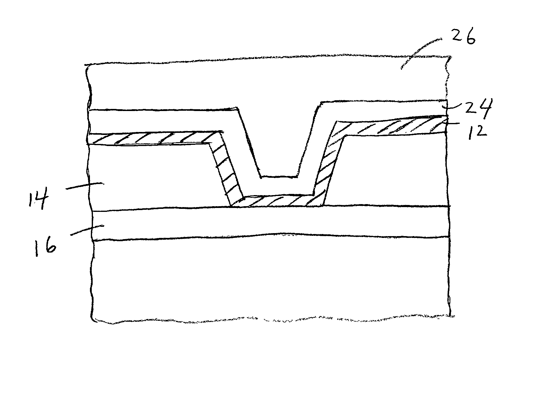
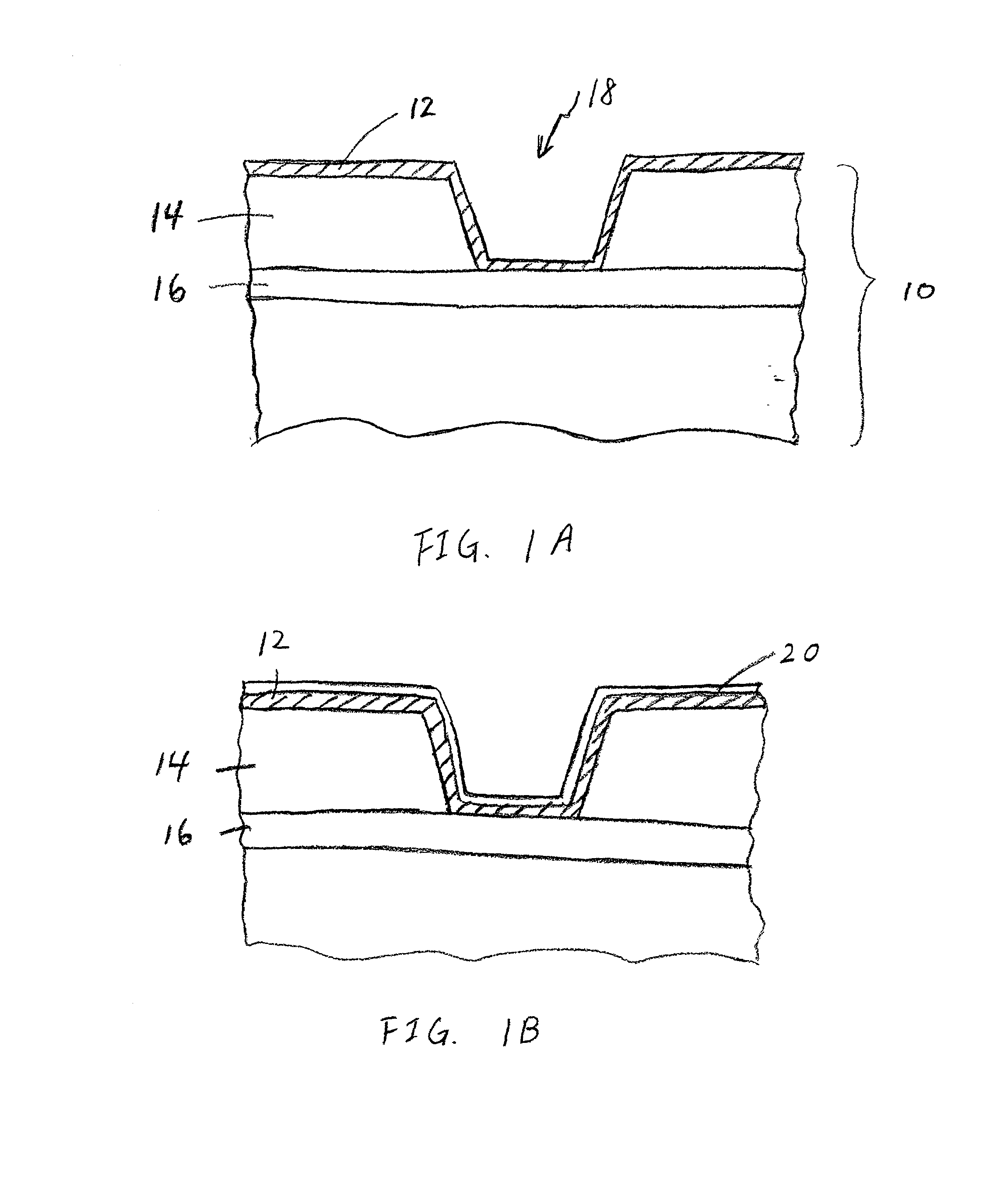
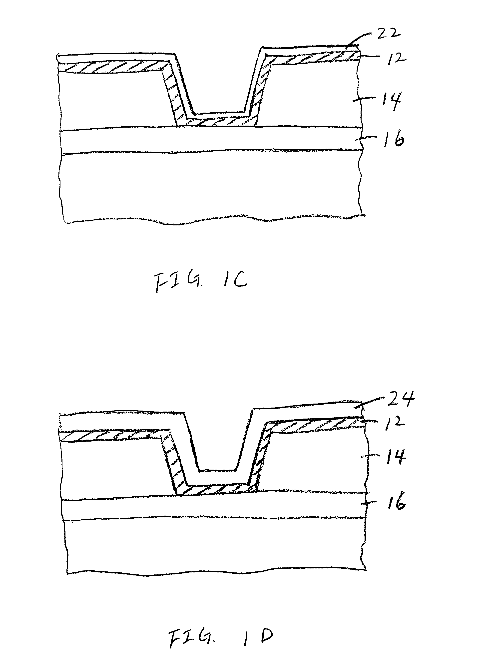
[0016] For illustration and exemplary purposes only, the following description of a specific embodiment of the invention pertains to a process for the formation of a tungsten nucleation layer. This specific process includes the use of a titanium-nitride (TiN) barrier layer as a metallic barrier layer, monosilane (SiH.sub.4) as the silicon-containing gas, and tungsten hexafluoride (WF.sub.6) as the refractory metal-containing gas. One skilled in the art will recognize, however, that processes according to the present invention are not limited to the use of a TiN barrier layer, ...


PUM

PropertyMeasurementUnit
thicknessaaaaaaaaaa
pressureaaaaaaaaaa
pressureaaaaaaaaaa

Abstract

A method for the formation of a refractory metal nucleation layer (e.g., a tungsten nucleation layer) on a semiconductor device substrate that includes first depositing a metallic barrier layer (e.g., a titanium-nitride barrier layer) on the substrate. Next, the metallic barrier layer is exposed to a silicon-containing gas (e.g., monosilane) to form a layer of silicon (e.g., a monolayer of silicon) on the metallic barrier layer. The layer of silicon is then exposed to a refractory metal-containing gas (e.g., WF6) in a manner such that the refractory metal-containing gas undergoes a reduction reaction with the layer of silicon. The result of this reaction is the formation of a refractory metal layer (e.g., a tungsten metal layer) on the metallic barrier layer. Subsequently, an alternating exposure of the refractory metal layer to the silicon-containing gas and the refractory metal-containing gas is conducted. This alternating exposure deposits additional refractory metal on the refractory metal layer in order to form a refractory metal nucleation layer. Processes according to the present invention employ a relatively high pressure (i.e., between 40 and 300 Torr) during formation of the tungsten nucleation layer. The relatively high pressure facilitates fast reactions and temperature stabilization during formation of the refractory metal nucleation layer and, thus, a high throughput process. In addition, the process can be combined with a conventional tungsten core layer deposition conducted at a relatively high pressure without the need to expend process time cycling between two different deposition pressures, thus providing a high effective throughput.

Description

[0001] 1. Field of the Invention[0002] The present invention, in general, relates to semiconductor device manufacturing methods and, in particular, to methods for the formation of refractory metal nucleation layers.[0003] 2. Description of the Related Art[0004] Semiconductor devices (e.g., silicon integrated circuits) often include metal interconnect structures that serve a variety of purposes, including carrying electrical signals between individual device elements, the provision of power, supplying a connection to ground and furnishing a connection to external apparatus. Such interconnect structures include horizontal patterned metal layers separated by intermetal dielectric (IMD) layers formed of, for example, silicon dioxide (SiO.sub.2). The horizontal patterned metal layers are connected by vertical metal interconnects (referred to as vias) formed in the IMD layer.[0005] One form of conventional via includes a titanium-nitride (TiN) barrier layer and a tungsten (W) core. The tu...

Claims


Application Information

Patent Timeline
Patent Type & Authority Applications(United States)
IPC IPC(8): H01L21/285H01L21/768
CPCH01L21/28556H01L21/28562H01L2221/1089H01L21/76876H01L21/76843
Inventor HERNER, SCOTT BRAD
Owner APPLIED MATERIALS INC
Why Eureka
Try Eureka