Microdevice having multilayer structure and method for fabricating the same

a multi-layer structure and micro-device technology, applied in the direction of 3d object support structures, fluid speed measurement, slide valves, etc., can solve the problems of poor productivity, long time, difficult to form, etc., and achieve the effect of easy formation of fine stoppers, thin flexible diaphragms, and excellent reproducibility

Inactive Publication Date: 2003-09-18
KAWAMURA INST OF CHEM RES
View PDF6 Cites 39 Cited by
  • Summary
  • Abstract
  • Description
  • Claims
  • Application Information

AI Technical Summary

Benefits of technology

0188] The present invention can provide a microdevice having a multi-layered structure comprising plural layers, particularly three or more layers having a cavity, a portion of which is used as a passage. Also, the present invention can provide a microdevice having a valve structure, which is capable of easily forming a fine stopper and a thin flexible diaphragm and bonding them to the desired position. Furthermore, it is made possible to obtain a device which causes neither clogging of a passage due to an adhesive nor leakage of liquid from the space between the respective layers or the space between the layer and another member. Furthermore, a chemical device, which causes neither adsorption nor loss of a biological component and exhibits excellent reproducibility, can be obtained by using an amphipathic polymerizable compound. Consequently, it is made possible to provide a microdevice which can perform complicated reaction and analysis processes.

Problems solved by technology

However, fixation by screw-screw-fastening is likely to cause leakage of a liquid between laminated base materials or between the base material and the cover, while fusion and bonding require a very long time, resulting in extremely poor productivity.
According to the material and method, it is difficult to form a microdevice having a multi-layered structure wherein passages and other void portions are formed continuously in three layers, and it is considerably difficult to form a microdevice wherein numerous fragile thin layers are laminated.
However, these two passages are independent passages and it was impossible to form thin capillary passages which pierce through the respective layers to communicate with each other.
It was particularly impossible to industrially manufacture a microdevice having a multi-layered structure composed of a layer, which is too thin to support itself, using a flexible material and it was also impossible to manufacture a microdevice which can perform complicated reaction and analysis processes.
Furthermore, there was a drawback in that the application is limited because the silicone rubber considerably adsorbs the biological substance and it requires a long time to cure the silicone rubber, resulting in extremely low productivity.
However, according to this method, it was difficult to laminate numerous films having a cut portion, which are too thin to support themselves while aligning the microcut portions from an industrial point of view.
Particularly, in the case in which the cut portion of the resin layer is in the form of a continuous line, a curve or numerous lines, it becomes more difficult to handle the film.
Also, there is no known microdevice obtained by laminating three or more films each having a cut portion, which are made of an active energy ray curable resin and are too thin to support themselves, while aligning the microcut portions.

Method used


Image

  • Microdevice having multilayer structure and method for fabricating the same
  • Microdevice having multilayer structure and method for fabricating the same
  • Microdevice having multilayer structure and method for fabricating the same

Examples


example 1

[0203] In this Example, a method of producing a microdevice of the present invention using an acrylic resin as the composition (x) by a method of peeling a coating substrate will be described.

[0204] Step (i)

[0205] As a coating substrate (1), a 30 .mu.m thick biaxially stretched polypropylene film (OPP film, manufactured by Futamura Chemical Industries Co., Ltd.), one surface of which is subjected to a corona discharge treatment was used after cutting into a size of 5 cm.times.5 cm. On the surface subjected to the corona treatment, the composition (x-1) was applied using a 127 .mu.m thick bar coater to form a coating film (2).
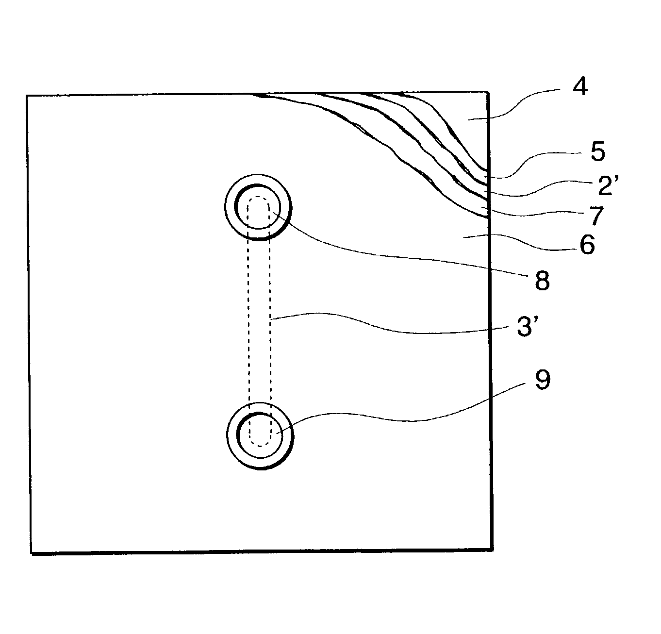
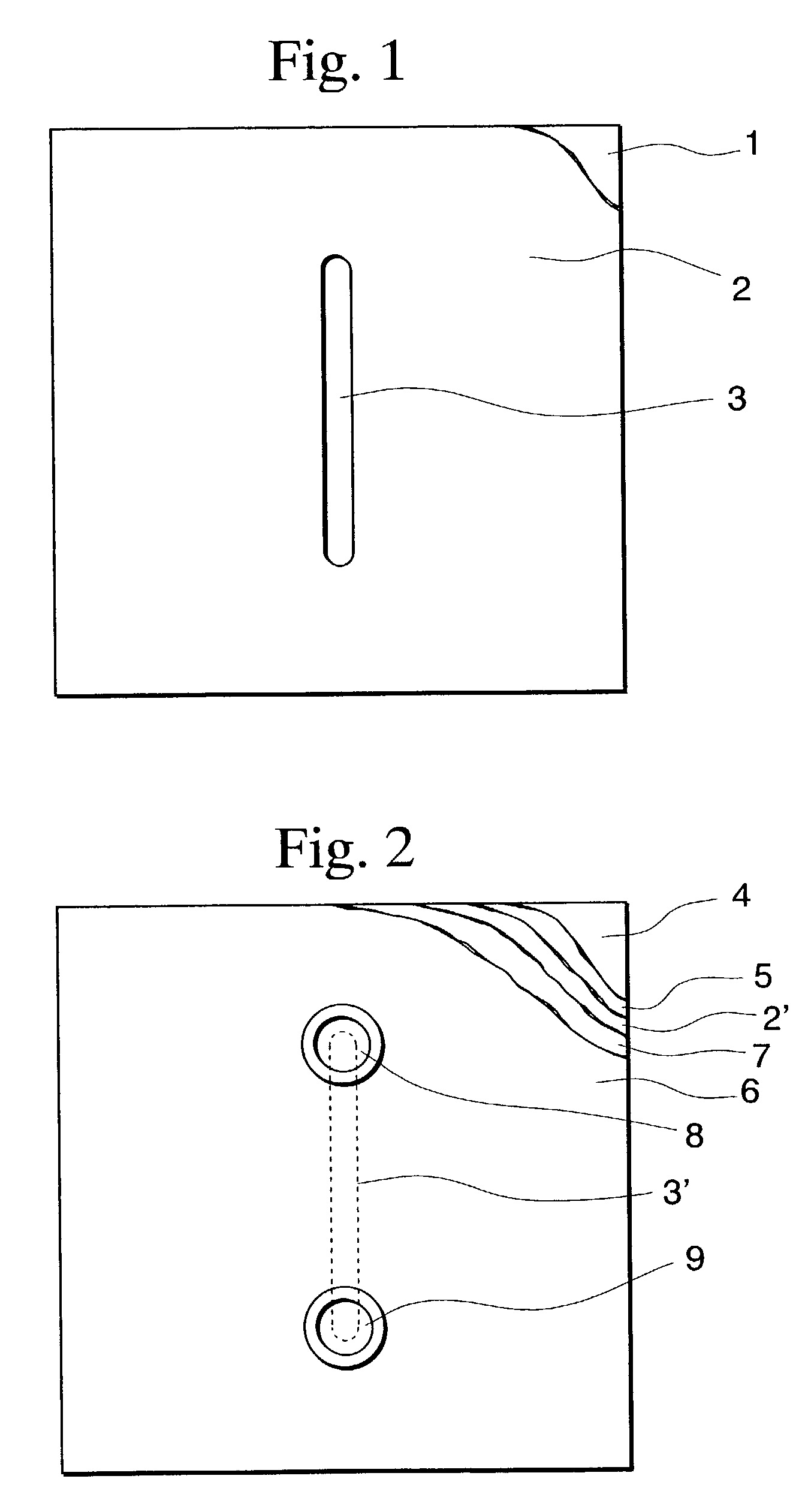
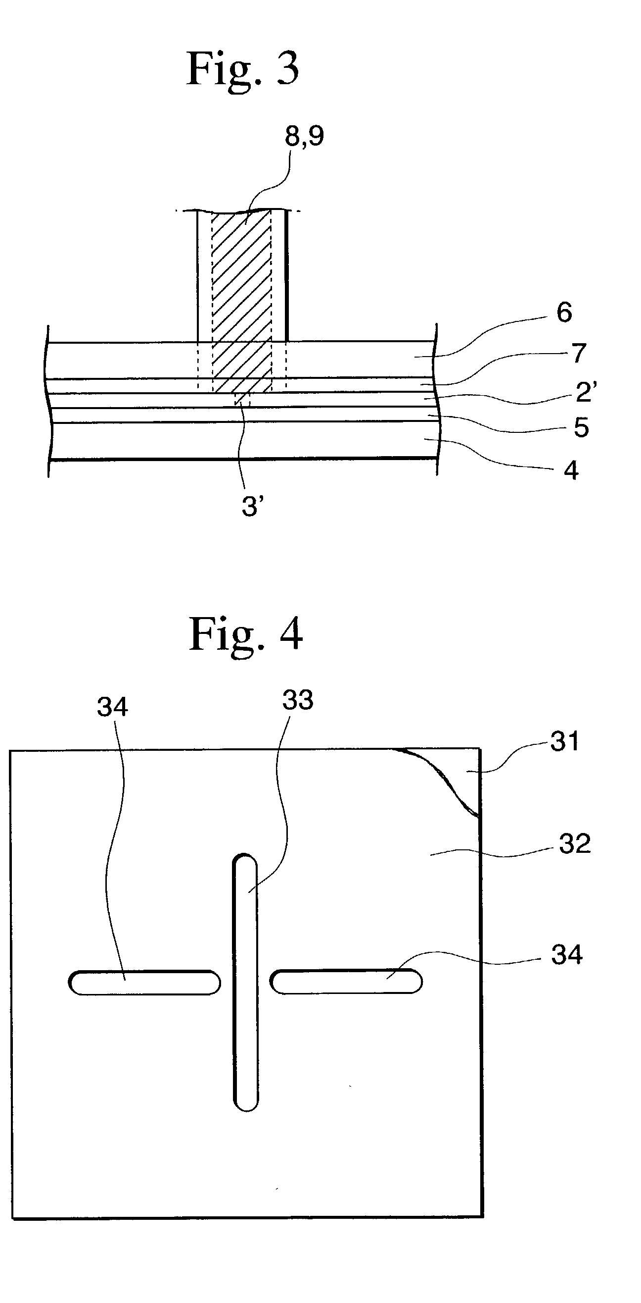
[0206] Step (ii)

[0207] In a nitrogen atmosphere, a portion other than a non-exposure portion (3) shown in FIG. 1 was irradiated with ultraviolet light via a photomask having a width of a non-exposure portion of 100 .mu.m and a length of a non-exposure portion of 30 mm for one second, thereby semi-curing the portion.

[0208] Step (iii)

[0209] While exposing the semi...

example 2

[0228] In this Example, the method of the present invention using a member (J) having a recessed cut portion on the surface will be described.

[0229] Manufacture of Member (J)

[0230] A member (J-2) was manufactured by interposing a plate having dimensions of 5 cm.times.5 cm.times.3 mm (thickness) made of polystyrene ("DICSTYRENE XC-520", manufactured by Dainippon Ink and Chemicals, Inc.) and a mold made of a silicon wafer between glass plates, fastening them with a spring clamp, heating in a hot-air oven at 120.degree. C. for about 2 hours, cooling to room temperature, removing the mold and the glass plates to form a groove-shaped recessed portion having the same shape and length as those in Example 1, except that a groove has a width of 50 .mu.m and a depth of 25 .mu.m, on the surface of a polystyrene plate.

[0231] Formation of Semi-Cured Coating Film

[0232] In the same manner as in Example 1, except that a pattern of exposure has a configuration such that each orifice having a diamete...

example 3

[0235] In this Example, a method of producing a microdevice of the present invention using a maleimide resin as the composition (x) by a method of peeling a coating substrate will be described. In the same manner as in Example 1, except that a composition (x-2) was used as the composition (x) in place of the composition (x-1) and a composition (x-2') was used in place of the composition (x-1') and, furthermore, the exposure time was 2 seconds, a microdevice (D-3) having the same structure as that in Example 1 was manufactured.


PUM

PropertyMeasurementUnit
thicknessaaaaaaaaaa
widthaaaaaaaaaa
contact angleaaaaaaaaaa

Abstract

The present invention provides a method of manufacturing a microdevice having a fine capillary cavity formed as a cut portion of a very thin layer which is likely to be broken, particularly a method of manufacturing a microdevice having complicated passages formed in three dimensions with high productivity. Also, the present invention provides a multi-functional microdevice which has a fine capillary passage formed by laminating plural resin layers, fine capillary cavities piercing through the respective layers to communicate and intersect three-dimensionally with each other, a space which should serve as a reaction chamber, a diaphragm valve, and a stopper structure. The method includes the steps of forming a semi-cured coating film having a cut portion made of an active energy ray curable composition on a coating substrate, laminating the semi-cured coating film with another member and removing the substrate, irradiating the semi-cured coating film again with an active energy ray before and/or after the removal of the substrate, thereby curing the coating film and bonding with said another member. The microdevice has a multi-layered structure wherein a member (J') {selected from a member having a cut portion piercing through the member, a member having a recessed cut portion on the surface, and a member having a cut portion piercing through the member and a recessed cut portion on the surface}, a member (K') and one or more active energy ray curable resin layers (X') having a cut portion at a portion of the layer, the cut portion having a minimum width within a range from 1 to 1000 mum, are laminated and two or more cut portions in the members are connected to form a cavity.

Description

[0001] The present invention relates to a method of manufacturing microdevices, for example, microfluidic device having a microfluid passage therein, a microreaction device (microreactor) which is to be used in extensive fields such as chemistry, biochemistry, and physical chemistry, or microprobe analytical device having a microcavity therein and a structure such as fluid passage, reaction chamber, electrophoresis column, membrane separation mechanism or sensor formed in a member, which is useful as an integrated DNA analytical device, microelectrophoresis device or microchromatography device; and relates to microdevices obtained by the method.[0002] More particularly, the present invention relates to a microdevice, which has a laminated structure comprising an active energy ray curable resin layer, the active energy ray curable resin layer having a cut portion of the resin in the layer, and has a fine capillary passage formed by laminating plural resin layers, the cut portions pie...

Claims


Application Information

Patent Timeline
Patent Type & Authority Applications(United States)
IPC IPC(8): B01J19/00B01L3/00B29C67/00B32B3/20B81B1/00
CPCB01J19/0093Y10T156/10B01J2219/00824B01J2219/00826B01J2219/00837B01J2219/00891B01L3/502707B01L2200/12B01L2300/0864B01L2300/0874B01L2300/0887B01L2400/0406B01L2400/0622B01L2400/0638B29C67/0066B29K2995/0073B29L2031/756B32B3/20B01J2219/00783B29C64/135B32B3/00
Inventor ANAZAWA, TAKANORITERAMAE, ATSUSHI
Owner KAWAMURA INST OF CHEM RES
Why Eureka
Try Eureka