

Cold cathode field emission device and process for the production thereof, and cold cathode field emission display and process for the production thereof
a technology of emission device and emission display, which is applied in the manufacture of electrode systems, discharge tubes with screens, and luminescent screens. it can solve the problems of increasing display production cost, difficult to achieve uniform formation, and difficulty in achieving a higher brightness and a larger screen siz
- Summary
- Abstract
- Description
- Claims
- Application Information
AI Technical Summary
Benefits of technology
Problems solved by technology
Method used
Image

Examples
example 2
[0324] Example 2 is concerned with the process for producing a field emission device according to the first-B aspect of the present invention and the process for producing a display according to the first-B aspect of the present invention, and also concerned with the field emission device and the display according to the first aspect of the present invention. The constitution and structure of the field emission device and display in Example 2 and such constitutions and structures in Examples 3 to 6 to be described later are substantially the same as those in Example 1, so that detailed explanations thereof will be omitted.
[0325] The processes for producing the field emission device and the display in Example 2 will be explained with reference to FIGS. 5A and 5B, FIGS. 6A and 6B and FIG. 7 hereinafter.
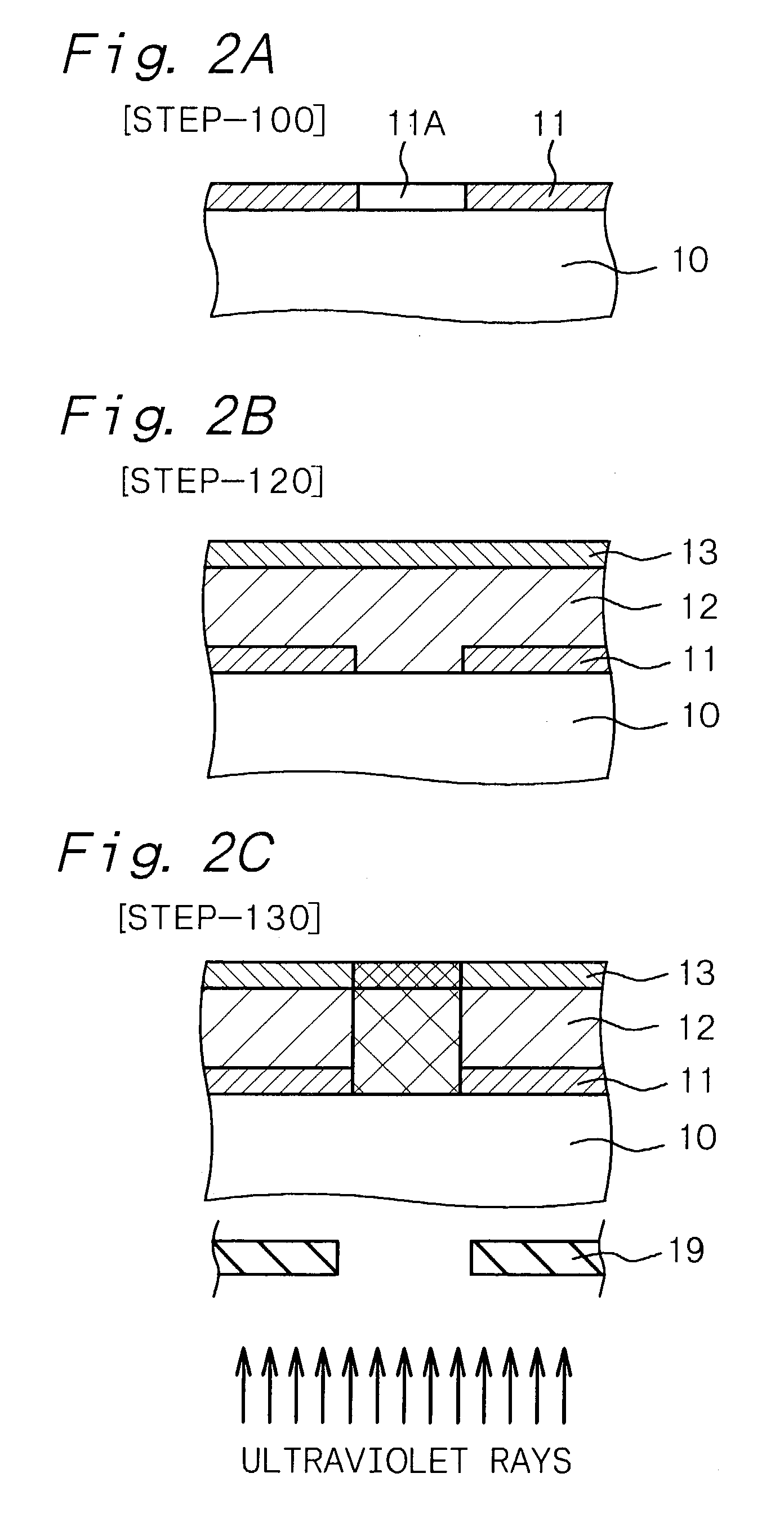
[0326] [Step-200]
[0327] First, the step of "forming a cathode electrode", the step of "forming an insulating layer composed of a photosensitive material that transmits exposure light", ...
example 3
[0343] Example 3 is concerned with the process for producing a field emission device according to the first-C aspect of the present invention and the process for producing a display according to the first-C aspect of the present invention. Further, it is concerned with the field emission device and the display according to the first aspect of the present invention.
[0344] The processes for producing the field emission device and the display in Example 3 will be explained with reference to FIGS. 8A and 8B and FIGS. 9A and 9B.
[0345] [Step-300]
[0346] First, the step of "forming a cathode electrode" is carried out in the same manner as in [Step-100] in Example 1.
[0347] [Step-310]
[0348] Then, an insulating layer 12A composed of a non-photosensitive material that transmits exposure light is formed on the entire surface. That is, the step of "forming an insulating layer composed of a non-photosensitive material that transmits exposure light" is carried out. The insulating layer 12A can be m...
example 4
[0361] Example 4 is concerned with the process for producing a field emission device according to the first-D aspect of the present invention and the process for producing a display according to the first-D aspect of the present invention, and it is further concerned with the field emission device and the display according to the first aspect of the present invention.
[0362] The processes for producing the field emission device and the display in Example 4 will be explained with reference to FIGS. 10A and 10B, FIGS. 11A and 11B, FIGS. 12A and 12B, FIGS. 13A and 13B and FIG. 14 hereinafter.
[0363] [Step-400]
[0364] First, [Step-100] of Example 1 (the step of "forming a cathode electrode"), [Step-310] of Example 3 (the step of "forming an insulating layer composed of a non-photosensitive material that transmits exposure light") and [Step-320] of Example 3 (the step of "forming a gate electrode composed of a non-photosensitive material") are carried out.
[0365] [Step-140]
[0366] Then, a fir...
PUM
 Abstract
Description
Claims
Application Information