Electron beam apparatus and a device manufacturing method by using said electron beam apparatus

a manufacturing method and electron beam technology, applied in the direction of beam/ray centering arrangement, semiconductor/solid-state device testing/measurement, instruments, etc., can solve the problems of not being able to apply to the electron beam apparatus without modification, the diameter of the objective lens may be further reduced, and the probability of oxide film breakdown is not negligibl

Inactive Publication Date: 2004-06-24
EBARA CORP
View PDF20 Cites 48 Cited by
  • Summary
  • Abstract
  • Description
  • Claims
  • Application Information

AI Technical Summary

Benefits of technology

0049] According to the third aspect of the second invention, the diameter of the objective lens may be further reduced, whereby a diameter of a optical column for accommodating the electron optical system can be made smaller.
0050] According to a fourth aspect of the second invention, a plurality of electron optical systems having the features of either one of the above described aspect is arranged in parallel above a sheet of sample. With this configuration, since different electron images for different regions on the sample

Problems solved by technology

Due to this, the use of the TaC chip has been problematic in that it can not be applied to the electron beam apparatus without modification.
In the prior-art defect inspection apparatus using the electron beam, however, there arises a problem that if the gate oxide film with a thickness of 1 nm or less is subjected to a relatively high dose level of electron beam, non-negligible probability of breakdown of the oxide film could be caused by the electron beam irradiation.
On the other hand, there has been a problem, however, that if the dose level of the electron beam is insufficient, a signal could not have sufficient S/N ratio in forming the image, which leads to a failure in accomplishing a highly reliable defect inspection.
However, there has been such a problem with the electron beam apparatus comprising the objective lens of the above-mentioned decelerating electric field type, in which a decelerating electric filed is produced between the objective lens and the wafer, that if the edge portion of the wafer is loca

Method used


Image

  • Electron beam apparatus and a device manufacturing method by using said electron beam apparatus
  • Electron beam apparatus and a device manufacturing method by using said electron beam apparatus
  • Electron beam apparatus and a device manufacturing method by using said electron beam apparatus

Examples


Embodiment Construction

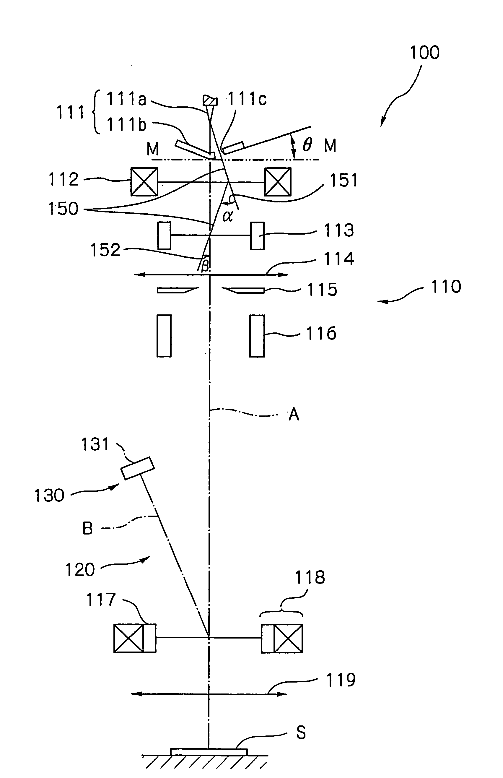
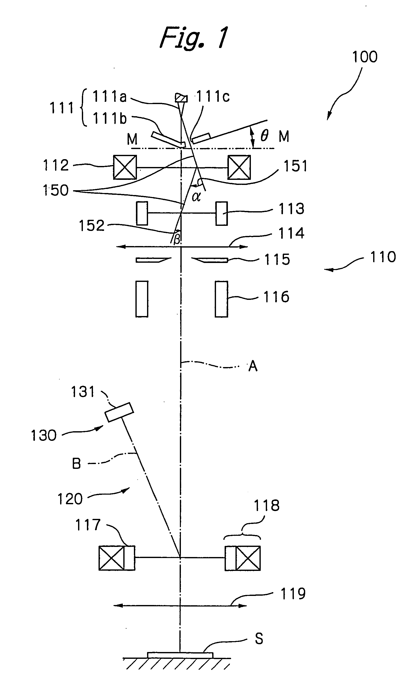
[0072] FIG. 1 schematically shows an electron beam apparatus 100 of an embodiment according to a first invention of the present invention. This electron beam apparatus 100 comprises a primary optical system 110, a secondary optical system 120 and an inspection unit 130. The primary optical system 110 is an optical system for irradiating an electron beam against a surface of a sample S (a sample surface), and comprises an electron gun 111 for emitting the electron beam, an electromagnetic deflector 112 and an electrostatic deflector 113 for deflecting the electron beam emitted from the electron gun, a condenser lens 114 for focusing the electron beam, an aperture 115 defining an numerical aperture, electrostatic deflectors 116 and 117 for controlling the electron beam so as to scan a surface of the sample, an E.times.B separator 118 and an objective lens 19, wherein those components described above are arranged along an optical axis "A" of the primary optical system 110 in a sequenti...


PUM


Abstract

An electron beam apparatus, in which an electron beam emitted from an electron gun having a cathode and an anode is focused and irradiated onto a sample, and secondary electrons emanated from the sample are directed into a detector, the apparatus further comprising means for optimizing irradiation of the electron beam emitted from the electron gun onto the sample, the optimizing means may be two-stage deflectors disposed in proximity to the electron gun which deflects and directs the electron beam emitted in a specific direction so as to be in alignment with the optical axis direction of the electron beam apparatus, the electron beam emitted in the specific direction being at a certain angle with respect to the optical axis due to the fact that, among the crystal orientations of said cathode, a specific crystal orientation allowing a higher level of electron beam emission out of alignment with the optical axis direction.

Description

[0001] The present invention relates to an electron beam apparatus and a device manufacturing method by using the electron beam apparatus, and more specifically to an electron beam apparatus which can evaluate a sample containing a device pattern having a minimum line width not greater than 0.1 .mu.m with high throughput and high reliability, and to a device manufacturing method which can improve a yield of products by using the electron beam apparatus to evaluate a wafer in the course of processing.DESCRIPTION OF THE RELATED ART AND PROBLEMS TO BE SOLVED BY THE INVENTION[0002] There has been suggested such an electron beam based inspection apparatus for inspecting defects in patterns formed on a surface of an object to be inspected, and more particularly, an inspection apparatus useful, for example, in inspecting defects on a wafer in a semiconductor manufacturing process, which includes irradiating an object to be inspected with an electron beam, detecting secondary electrons whic...

Claims


Application Information

Patent Timeline
IPC IPC(8): G01N23/225H01J3/02H01J3/10H01J37/04H01J37/06H01J37/063H01J37/073H01J37/12H01J37/147H01J37/28H01J37/317H01L21/66
CPCB82Y10/00B82Y40/00G01N23/225H01J3/021H01J3/10H01J2237/2817H01J37/073H01J37/1471H01J37/1472H01J37/3174H01J2237/06316H01J37/063
Inventor NAKASUJI, MAMORUKATO, TAKAONOJI, NOBUHARUSATAKE, TOHRUMURAKAMI, TAKESHIWATANABE, KENJI
Owner EBARA CORP
Why Eureka
Try Eureka