Rapid energy transfer annealing device and process

Inactive Publication Date: 2004-07-29
JIANG YEU LONG
View PDF0 Cites 42 Cited by
  • Summary
  • Abstract
  • Description
  • Claims
  • Application Information

AI Technical Summary

Benefits of technology

0026] It is an object of this invention to provide a rapid energy transfer annealing device and process allowing easy and large-area fabrication and capable of ef

Problems solved by technology

However, such temperature exceeding 600.degree. C. and the annealing time lasting for tens of seconds surpasses the softening temperature of the glass for too long time and thus may easily cause damages to the glass substrate.
However, comparing the near-UV photons emitted from excimer lasers, the absorption of near-IR photons emitted by the tungsten halogen lamp is poor due to the low absorption coefficients of all the amorphous silicon film layer, silicon dioxide layer, and glass substrate.
Therefore, the annealing effects generated by directly irradiating near-IR photons towards the amorphous silicon film layer in the conventional rapid thermal annealing (RTA) and pulsed rapid thermal annealing (PRTA) processes are not effective.
However, the absorption of near-IR photons emitted by the tungsten halogen lamp is poor due to the low absorption coefficients of all the amorphous silicon film layer, silicon dioxide layer, and glass substrate.
Further, the

Method used


Image

  • Rapid energy transfer annealing device and process
  • Rapid energy transfer annealing device and process
  • Rapid energy transfer annealing device and process

Examples


first embodiment

The First Embodiment

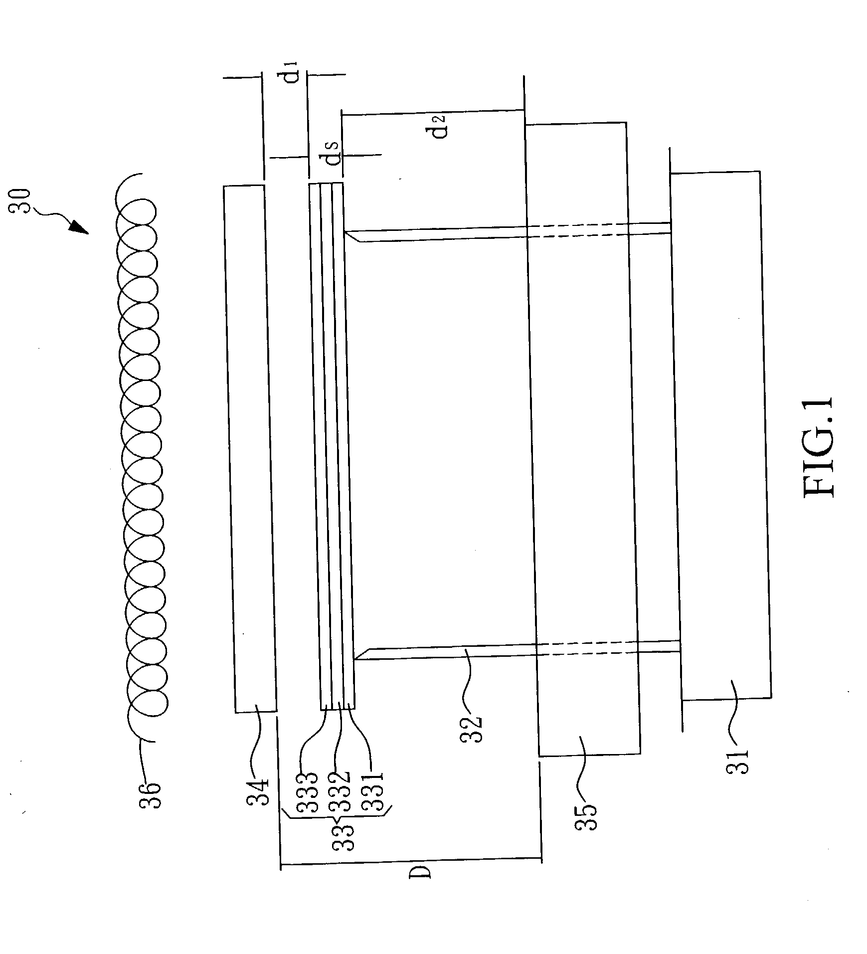
[0045] FIG. 1 is a schematic drawing of a first embodiment of the rapid energy transfer annealing device 30 according to this invention. The device 30 comprises a plurality of quartz pillars 32 affixed on a supporting plate 3 1; a sample 33 supported by the plurality of quartz pillars 32 and having a thickness of d.sub.S, the sample 33 including a glass substrate 331, a silicon dioxide layer 332 and an amorphous silicon film layer 333 sequentially deposited above the glass substrate 331; an energy plate 34 provided above the sample 33 at a first distance d.sub.1; a heat sink plate 35 provided below the sample 33 at a second distance d.sub.2 and allowing the plurality of quartz pillars 32 to pass through, such that the supporting plate 31 is capable of vertical movement; and a tungsten halogen lamp 36 provided above the energy plate 34 to supply photon energy required by the energy plate 34. The energy plate 34 is selected from the group consisting of graphite, mo...

second embodiment

The Second Embodiment

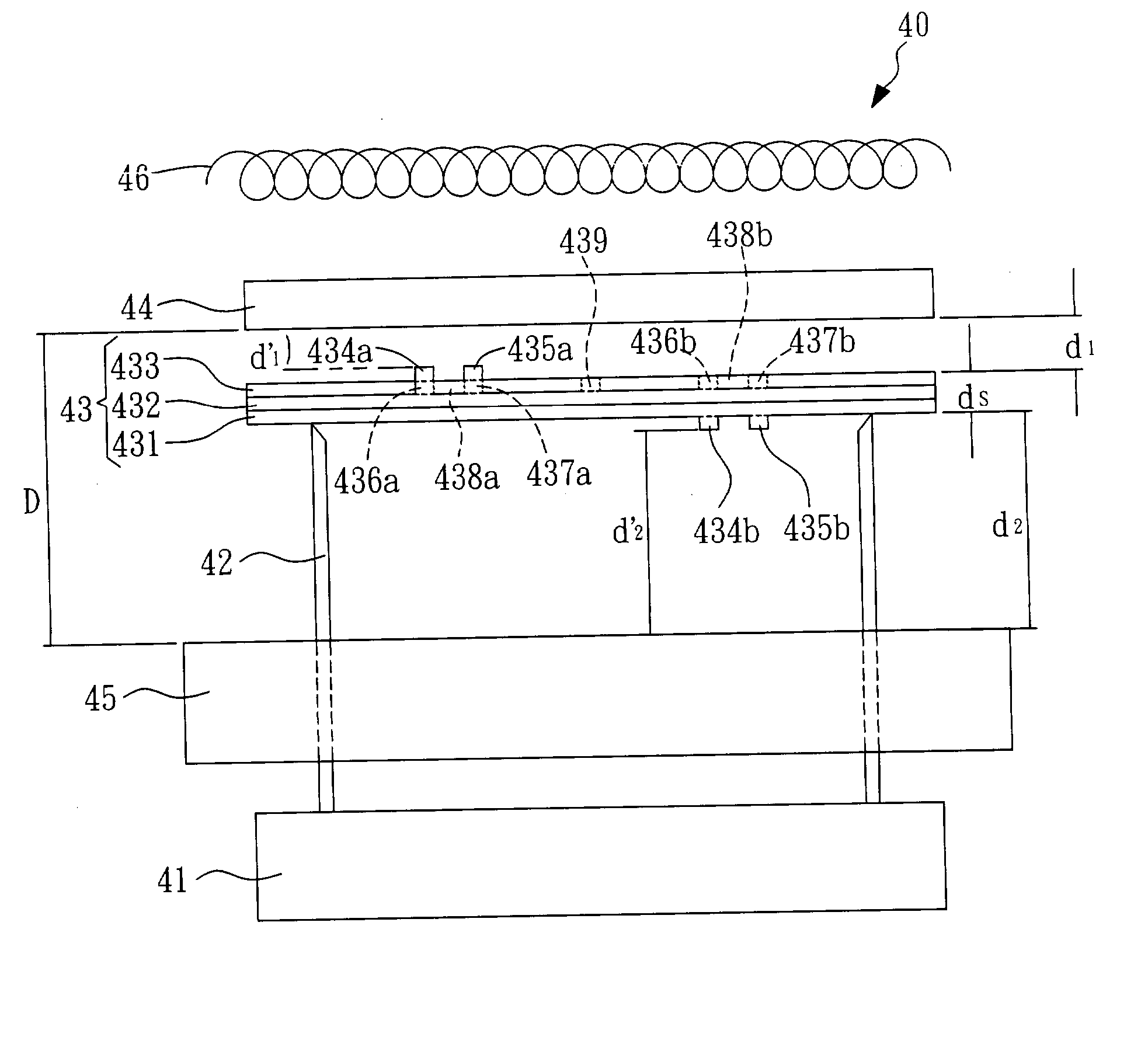
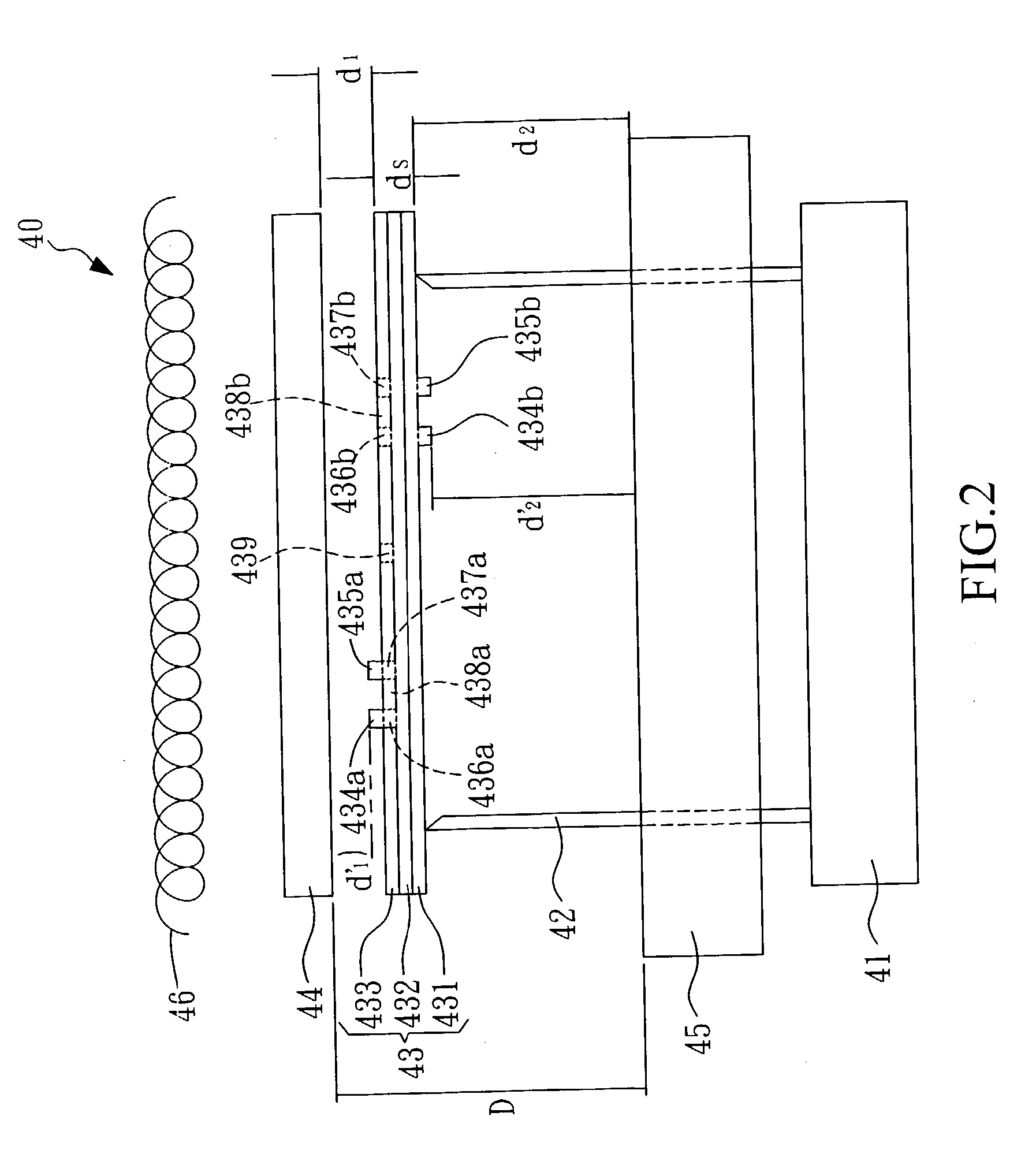
[0047] FIG. 2 is a schematic drawing of a second embodiment of the rapid energy transfer annealing device 40 according to this invention. The device 40 comprises a tungsten halogen lamp 46; a sample 43 having a thickness of d.sub.S, the sample including a glass substrate 431, a silicon dioxide layer 432 and a amorphous silicon film layer 433 sequentially deposited above the glass substrate 431; an energy plate 44 provided above the sample 43 at a first distance d.sub.1; and a heat sink plate 45 provided below the sample 43 at a second distance d.sub.2. The overall structure of this embodiment is substantially the same as that of the rapid energy transfer annealing device 30 of the first embodiment. The first distinguishable feature is a first high relief 434a on the amorphous silicon film layer 433. The protrusion of the first high relief 434a subjects its distance d.sub.1' with respect to the energy plate 44 is less than the first distance d.sub.1 between the a...

third embodiment

The Third Embodiment

[0048] FIG. 3 is a schematic drawing of a third embodiment of the rapid energy transfer annealing device 50 according to this invention. The structure and application of the device 50 are substantially the same as those of the rapid energy transfer annealing device 30 of the first embodiment. The device 50 comprises a tungsten halogen lamp 56 and an energy plate 54 that are both stationary. The distinguishable features in FIG. 3 are that a heat sink plate 55, a plurality of quartz pillars 52 affixed on a supporting plate 5 1, a sample 53 supported by the plurality of quartz pillars 52, and a heat sink( plate 55 located below the sample 53 are all placed on a conveyor (not shown) so as to move leftwards simultaneously. Hence, the sample 53 may pass beneath the energy plate 54 along with the conveyor. By the heat scan released by the energy plate 54, the heat released by the energy plate 54 is rapidly absorbed so as to allow rapid temperature elevation. The heat si...


PUM


Abstract

Disclosed is a rapid energy transfer annealing (RETA) device and process, where an energy plate is used to rapidly absorb the primary photonic energy of the light source, such as a tungsten halogen lamp (or an xenon Arc lamp), to allow temperature elevation. The energy plate faces an amorphous thin film deposited above a glass or plastic substrate and releases the heat energy transferred by a gas or solid medium to the amorphous thin film,, so as to heat the amorphous thin film for transforming the amorphous thin film into a polycrystalline film. On another side of the glass or plastic substrate may be further provided with a heat sink plate and a supporting plate. The heat sink plate absorbs energy of the glass substrate, protects glass substrate from damages due to overheating. The heat sink plate or the supporting plate may be moved to freely adjust distance between the amorphous thin film and the energy plate and that between the glass substrate and the heat sink plate, so as to control energy transferred to the amorphous thin film and energy released by the glass substrate transfer. The adjustment of distance may be fixed or varied as a function of time so as to randomly adjust the energy transfer. Further, between the glass substrate and the amorphous film may be provided with a heat conducting layer and a heat shielding layer. On another side of the glass substrate may be provided with a heat sink layer. On the amorphous thin film may be provided with a heat absorption layer to control and allow selective crystallization, or to control direction of heat transfer thereby guiding the crystallization to grow in a specific direction.

Description

[0001] This invention is related to a rapid energy transfer annealing device and process, in particular to one having an energy plate capable of rapidly absorbing photonic energy, elevating temperature and releasing heat energy, and a heat sink plate capable of controlling temperature.BACKGROUND OF INVENTION[0002] Increasing the driving speed of Thin Film Transistor (TFT) and improving the stability and conversion efficiency of amorphous silicon thin film solar cell are the basic requirements for the new generation TFT flat panel display and Thin Film Solar Cell. Because low temperature polysilicon (LTPS) may be integrated into a glass or a plastic substrate, and consists of electron mobility being one to two orders of magnitude higher than amorphous silicon, it can effectively improve the mobility of TFT and the stability and conversion efficiency of Thin Film Solar Cell. The LTPS has become an important material for fabricating the high driving speed of a new generation TFT flat p...

Claims


Application Information

Patent Timeline
IPC IPC(8): H01L21/00H01L21/20H01L21/324H01L31/18H02N6/00
CPCH01L21/2022H01L21/324Y02E10/50H01L31/1872H01L21/67115Y02P70/50H01L21/0242H01L21/02691H01L21/02488H01L21/02422H01L21/02532H01L21/02667H01L21/02595
Inventor JIANG, YEU-LONG
Owner JIANG YEU LONG
Why Eureka
Try Eureka