Organic dye-sensitized metal oxide semiconductor electrode and its manufacturing method, and organic dye-sensitized solar cell

a metal oxide semiconductor and manufacturing method technology, applied in the direction of electrolytic capacitors, thermoelectric devices, electrochemical generators, etc., can solve the problems of small practical use of solar cells, high price of solar cells using silicon as photoelectric conversion materials, and low pri

Inactive Publication Date: 2004-12-09
BRIDGESTONE CORP
View PDF3 Cites 49 Cited by
  • Summary
  • Abstract
  • Description
  • Claims
  • Application Information

AI Technical Summary

Problems solved by technology

However, a large amount of energy is required to form the crystalline silicon or the like and therefore the use of silicon brings about effect contrary to the original object of the solar cell, that is energy saving cell utilizing the sunlight.
Further as a result of the consumption of a large amount of energy, the solar cell using the silicon as a photoelectric conversion material becomes expensive.
25 .mu.A, and therefore it is little possible to put the solar cell to practical use.
However, in contrast with the solar cell using silicon, the semiconductor of metal oxide and organic dye used in this solar cell are manufactured in large quantity and the they are relatively at low price.
The above-mentioned solar cells do not show practically satisfactory electric current/voltage curve.
However, the fluorine-doped tin oxide has poor electrical conductivity and further is not adequate for a use (e.g., solar cell) requiring a large area.
However, even this transparent electrode of ITO does not have sufficiently reduced electri

Method used


Image

  • Organic dye-sensitized metal oxide semiconductor electrode and its manufacturing method, and organic dye-sensitized solar cell
  • Organic dye-sensitized metal oxide semiconductor electrode and its manufacturing method, and organic dye-sensitized solar cell
  • Organic dye-sensitized metal oxide semiconductor electrode and its manufacturing method, and organic dye-sensitized solar cell

Examples


example 1

[0133] (1) Preparation of Transparent Electrode

[0134] The transparent electrode was prepared using a sputtering device as follows:

[0135] Sputtering was carried out on a glass plate (thickness: 2 mm) of a size of 5.times.5 cm using a ceramic target of ITO (Indium-tin oxide) having 100 mm.phi. with flowing Ar gas of 10 cc / min. and oxygen gas of 1.5 cc / min. for five minutes under the conditions of pressure within the device of 5 mTorr and supply electric power of 500 W. Thus the ITO layer having the thickness of 3,000 .ANG. was formed on the glass plate, which had surface resistivity of 10 .OMEGA. / .quadrature..

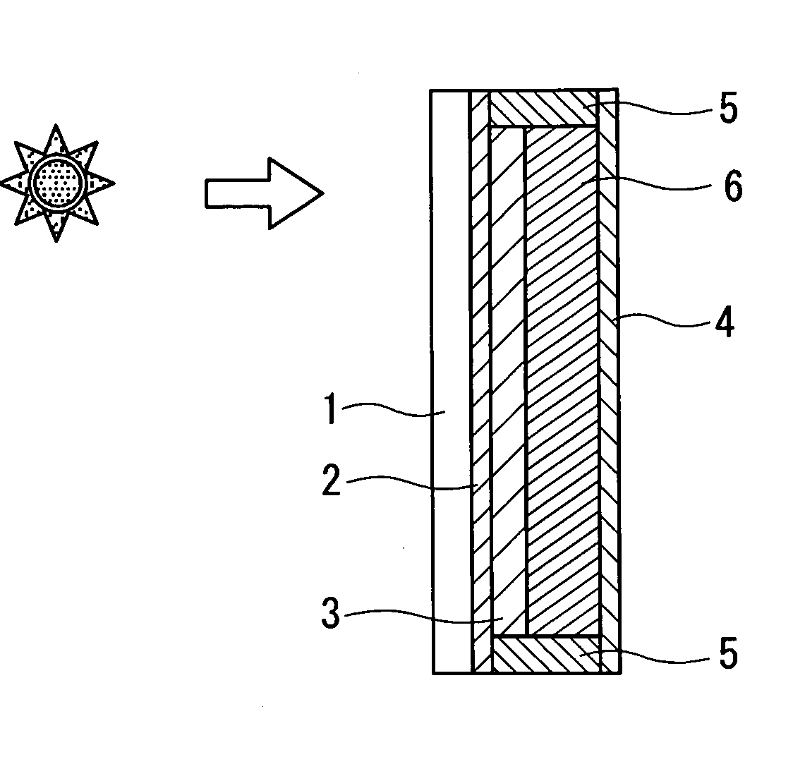
[0136] (2) Preparation of Semiconductor Layer of Metal Oxide

[0137] A titanium oxide thin layer was formed on the resultant glass plate provided with ITO transparent electrode using an electron beam heating type-vacuum deposition device as follows: A titanium oxide pellet having the purity of 99.99% was placed in a deposition source for an electron beam, and deposition was carried...

example 2

[0143] The procedure of Example 1 was repeated except for carrying out the preparation of semiconductor layer of metal oxide in the following manner to prepare a solar cell:

[0144] (2) Preparation of Semiconductor Layer of Metal Oxide

[0145] A titanium oxide thin layer was formed on the resultant glass plate provided with ITO transparent electrode using an electron beam heating type-vacuum deposition device as follows: A titanium oxide pellet having the purity of 99.99% was placed in a deposition source for an electron beam, and deposition was carried out under the condition of electric current of 250 mA to form a titanium oxide layer having the thickness of 3,000 .ANG.. The glass plate having the titanium oxide layer was further subjected to heat treatment at 500.degree. C. for 30 minutes.

[0146] The resultant solar cell was exposed to light having intensity of 100 W / cm.sup.2 by a solar simulator. As a result, Voc (voltage in open-circuit) was 0.61V, Joc (electric current density caus...

example 3

Opposed Target Type-dipole Sputtering

[0152] (1) Preparation of Transparent Electrode

[0153] The transparent electrode was prepared using a sputtering device as follows:

[0154] Sputtering was carried out on a glass plate (thickness: 2 mm) of a size of 5.times.5 cm using a ceramic target of ITO (Indium-tin oxide) having 100 mm.phi. with flowing Ar gas of 10 cc / min. and oxygen gas of 1.5 cc / min. for five minutes under the conditions of pressure within the device of 5 mTorr and electric power of 500 W. Thus the ITO layer having the thickness of 3,000 .ANG. was formed on the glass plate, which had surface resistivity of 10 .OMEGA. / .quadrature..

[0155] (2) Preparation of Semiconductor Layer of Metal Oxide

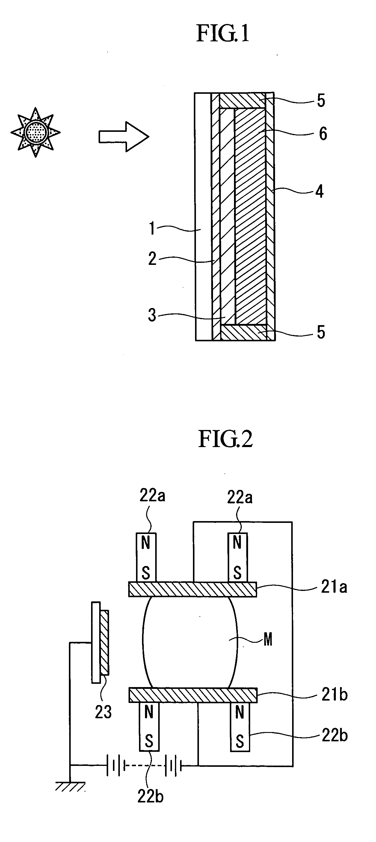
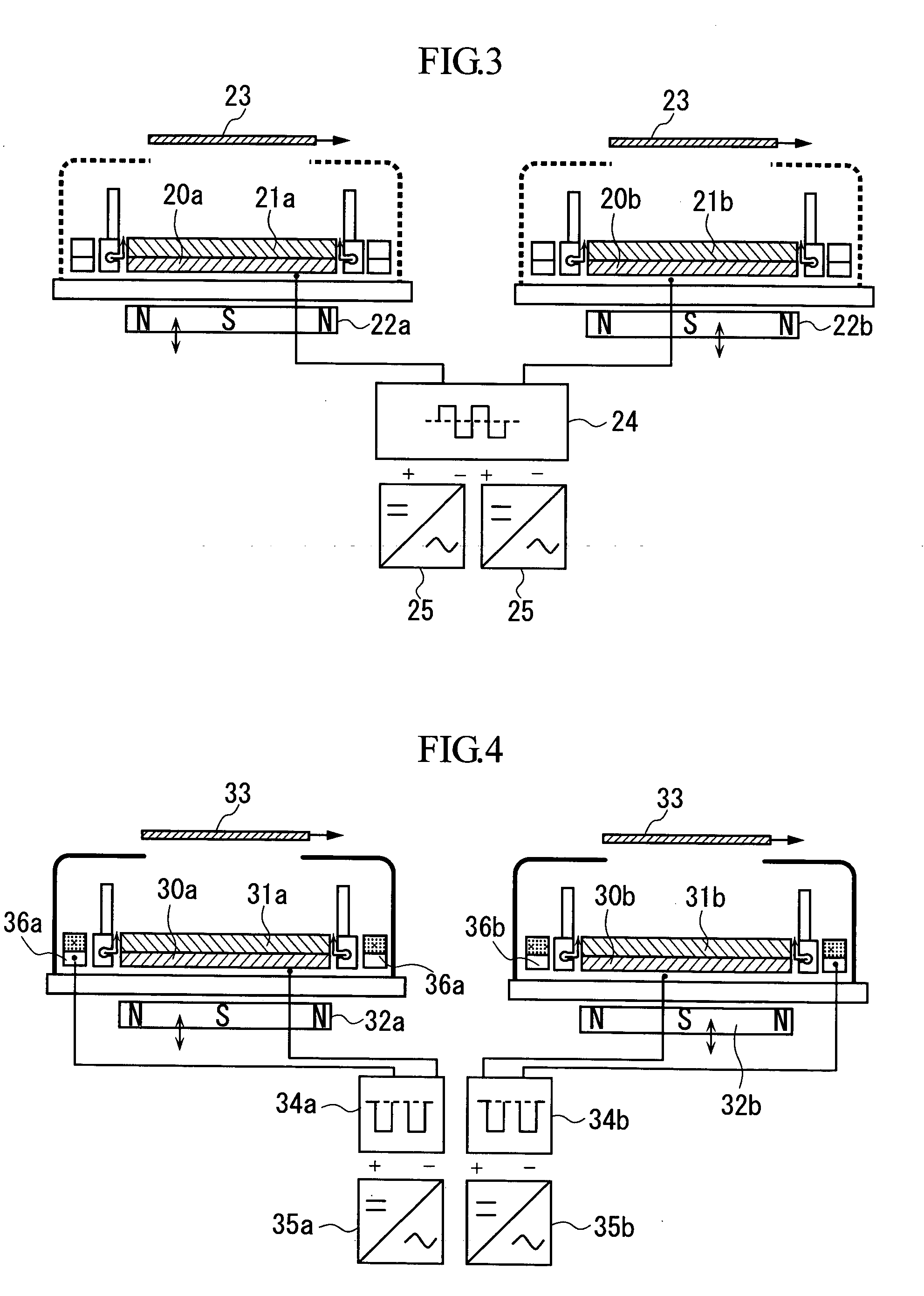
[0156] A titanium oxide thin layer was formed on the resultant glass plate provided with ITO transparent electrode using an opposed target type diode sputtering device shown in FIG. 2 as follows: Two sheets of metal titanium targets having diameter of 100 mm were placed above the glass plate...


PUM

PropertyMeasurementUnit
Fractionaaaaaaaaaa
Thicknessaaaaaaaaaa
Surface roughnessaaaaaaaaaa

Abstract

The present invention provides a semiconductor electrode of organic dye-sensitized metal oxide having a semiconductor layer of metal oxide that can be easily prepared, and an organic dye-sensitized solar cell. The semiconductor electrode of organic dye-sensitized metal oxide comprises a substrate having a transparent electrode thereon, a semiconductor layer of metal oxide provided on the electrode and an organic dye absorbed on a surface of the semiconductor layer, the semiconductor layer being formed by a vapor deposition process.

Description

BACKGROUND OF INVENTION[0001] 1. Field of the Invention[0002] The present invention relates to an organic dye-sensitized solar cell, a semiconductor electrode of organic dye-sensitized metal oxide advantageously used in the solar cell and the process for the preparation thereof.[0003] 2. Description of the Related Art[0004] Recently, great attention has been paid to a solar cell that converting directly the sunlight to electrical energy from the standpoints of energy saving, effective utilization of resources and prevention of environmental pollution, and therefore the development of the solar cell has been advanced.[0005] As the solar cell, those utilizing crystalline silicon or amorphous silicon widely employed. However, a large amount of energy is required to form the crystalline silicon or the like and therefore the use of silicon brings about effect contrary to the original object of the solar cell, that is energy saving cell utilizing the sunlight. Further as a result of the c...

Claims


Application Information

Patent Timeline
IPC IPC(8): C23C14/08H01G9/20H01M14/00
CPCC23C14/08H01G9/2031H01G9/2059H01M14/005Y02E10/542
Inventor KOBAYASHI, TAICHIYOSHIKAWA, MASATOIWABUCHI, YOSHINORITANUMA, ITSUOOONO, SHINGO
Owner BRIDGESTONE CORP
Why Eureka
Try Eureka