Laser irradiation apparatus and method of fabricating semiconductor device

a laser irradiation and semiconductor technology, applied in the direction of manufacturing tools, energy-based chemical/physical/physico-chemical processes, transistors, etc., can solve the problems of lowering productivity, affecting the efficiency of semiconductor devices, and affecting the surface of semiconductor films

Inactive Publication Date: 2004-12-23
SEMICON ENERGY LAB CO LTD
View PDF18 Cites 50 Cited by
  • Summary
  • Abstract
  • Description
  • Claims
  • Application Information

AI Technical Summary

Benefits of technology

[0015] In view of the problem described above, it is an object of the present invention to provide a laser irradiation apparatus being able to suppress the unevenness of the crystallinity or the state of the surface of the semiconductor film and to perform homogeneous crystallization of the semiconductor film. It is another object of the present invention to provide a method for manufacturing a semiconductor device with the use of the laser irradiation apparatus being able to suppress the variation of the on-current, the mobility, and the threshold of TFT.

Problems solved by technology

Moreover, when the semiconductor film is crystallized by the irradiation of the laser light in the atmosphere, the surface of the semiconductor film becomes somewhat rough.
Therefore, when the state of the surface of the semiconductor film becomes uneven due to the energy fluctuation of the laser light, the interface state density at the interface between the semiconductor film and the gate insulating film formed afterward varies, which results in the variation of the threshold of TFT.
When the energy of the laser light decreases, the throughput in the crystallization also decreases, which results in the lowering of the productivity.
Moreover, since the non-linear optical element is easy to deteriorate due to the laser light and is inferior in endurance, when the energy of the fundamental wave is increased in order to obtain the laser light of the harmonic having high energy, it is necessary to do the maintenance frequently.

Method used


Image

  • Laser irradiation apparatus and method of fabricating semiconductor device
  • Laser irradiation apparatus and method of fabricating semiconductor device
  • Laser irradiation apparatus and method of fabricating semiconductor device

Examples


embodiment 1

[0217] Embodiment 1

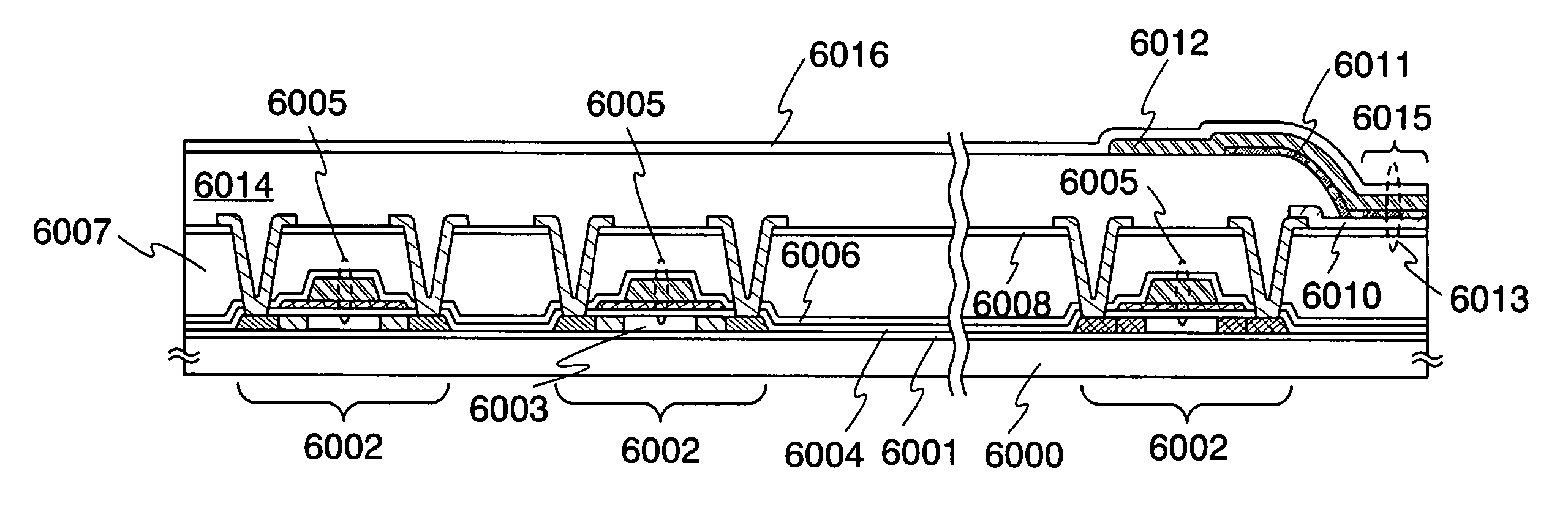
[0218] A structure of the pixel in the light-emitting device, one of the semiconductor devices formed using the laser irradiation apparatus of the present invention, is explained with reference to FIG. 10.

[0219] In FIG. 10, a base film 6001 is formed over a substrate 6000 and a transistor 6002 is formed over the base film 6001. The transistor 6002 has an active layer 6003, a gate electrode 6005, and a gate insulating film 6004 sandwiched between the active layer 6003 and the gate electrode 6005.

[0220] A polycrystalline semiconductor film crystallized using the laser irradiation apparatus of the present invention is used as the active layer 6003. It is noted that not only silicon but also silicon germanium may be employed as the active layer. When the silicon germanium is employed, it is preferable that the concentration of germanium is in the range of 0.01 atomic % to 4.5 atomic %. Alternatively silicon with carbon nitride added may be also employed.

[0221] Silicon...

embodiment 2

[0241] Embodiment 2

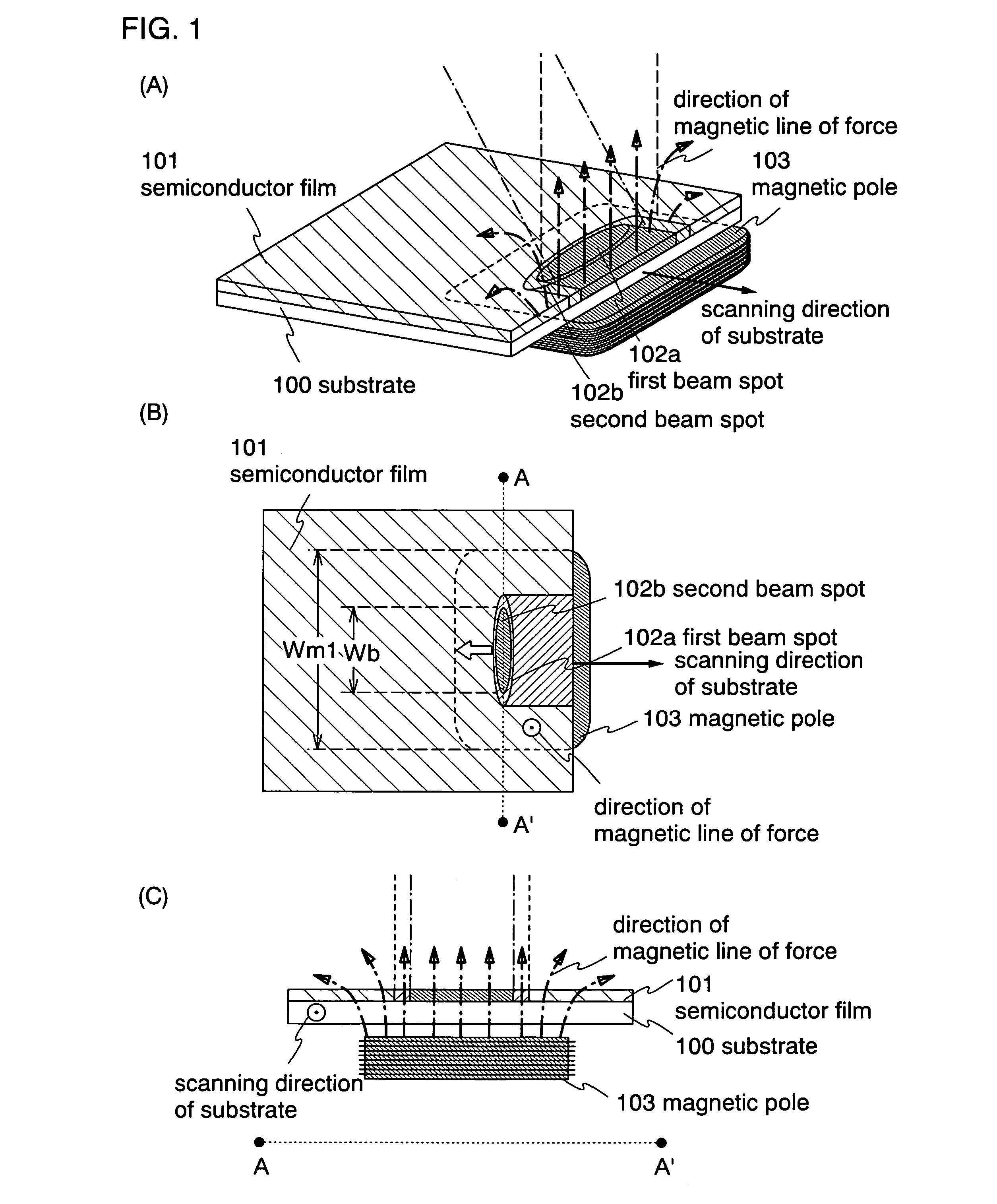
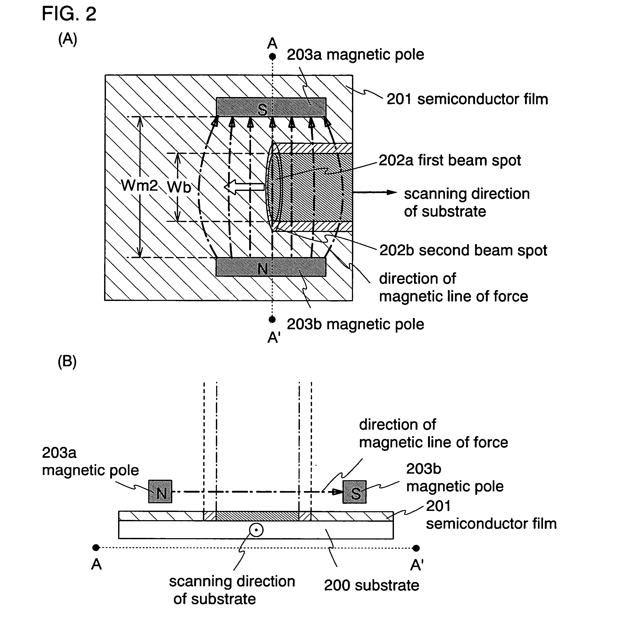
[0242] This embodiment explains a shape of the first beam spot obtained by combining a plurality of the first laser light shown in FIG. 4(B). It is noted that the first beam spot is referred to as a beam spot simply in this embodiment.

[0243] FIG. 11(A) shows an example of the shape of the beam spot of the laser light oscillated from each of a plurality of laser oscillators on a processed object. The beam spot shown in FIG. 11(A) is elliptical in shape. It is noted that the shape of the beam spot of the laser light oscillated from the laser oscillator is not limited to elliptical in the present invention. The shape of the beam spot depends on the kind of the laser, and the shape thereof can be changed through an optical system. For example, the laser light emitted from the excimer laser L3308 manufactured by Lambda Physik, Inc. (wavelength 308 nm, pulse with 30 ns) is rectangular in shape having a size of 10 mm.times.30 mm (both are width at half maximum in a beam ...


PUM

PropertyMeasurementUnit
magnetic fieldaaaaaaaaaa
wavelengthaaaaaaaaaa
magnetic flux densityaaaaaaaaaa

Abstract

According to the present invention, oxygen and nitrogen are effectively prevented from mixing into the semiconductor film by doping Ar or the like in the semiconductor film in advance, and by irradiating the laser light in the atmosphere of Ar or the like. Therefore, the variation of the impurity concentration due to the fluctuation of the energy density can be suppressed and the variation of the mobility of the semiconductor film can be also suppressed. Moreover, in TFT formed with the semiconductor film, the variation of the on-current in addition to the mobility can be also suppressed. Furthermore, in the present invention, the first laser light converted into the harmonic easily absorbed in the semiconductor film is irradiated to melt the semiconductor film and to increase the absorption coefficient of the fundamental wave.

Description

[0001] 1. Technical Field of the Invention[0002] The present invention relates to a continuous wave laser irradiation apparatus utilized for crystallizing a semiconductor film. In addition, the present invention relates to a method for manufacturing a semiconductor device including a process for crystallizing the semiconductor film with the use of the laser irradiation apparatus.[0003] 2. Description of the Related Art[0004] A thin film transistor using a polycrystalline semiconductor film (polycrystalline TFT) is superior to TFT using an amorphous semiconductor film in its mobility by double digits or more and has an advantage that a pixel portion and its peripheral driver circuit in a semiconductor display device can be integrally formed on the same substrate.[0005] The polycrystalline semiconductor film can be formed over an inexpensive glass substrate when a laser annealing method is employed. However, the energy of the laser light output from the oscillator fluctuates by at lea...

Claims


Application Information

Patent Timeline
Patent Type & Authority Applications(United States)
IPC IPC(8): B01J19/08B01J19/12B23K26/12H01L21/20H01L21/265H01L21/268H01L21/336H01L29/786
CPCB23K26/0604B23K26/0608B23K26/0639B23K26/0643B23K26/0648B23K26/0665B23K26/12B23K26/123H01L21/2026H01L21/268H01L29/66757B23K26/127B23K26/064H01L21/02425H01L21/02683H01L21/02686H01L21/02678H01L21/02422H01L21/02532H01L21/0242H01L21/02691
Inventor YAMAZAKI, SHUNPEINAKAMURA, OSAMUSHOJI, HIRONOBUTANAKA, KOICHIRO
Owner SEMICON ENERGY LAB CO LTD
Why Eureka
Try Eureka