System and method for performing sputter etching using independent ion and electron sources and a substrate biased with an a-symmetric bi-polar DC pulse signal

a sputter etching and independent ion and electron source technology, applied in the direction of electrolysis components, vacuum evaporation coatings, coatings, etc., can solve the problems of limiting the control of ion energies at the etched surface, high gas pressure, and low electrode voltage, so as to optimize the etching performance

Inactive Publication Date: 2005-01-13
4WAVE
View PDF4 Cites 20 Cited by
  • Summary
  • Abstract
  • Description
  • Claims
  • Application Information

AI Technical Summary

Benefits of technology

The present invention is directed to a system for performing sputter etching. Biasing circuitry biases a substrate with an a-symmetric bi-polar DC voltage pulse signal. The biasing circuitry is formed from a positive voltage source with respect to ground, a negative voltage source with respect to ground and a high frequency switch. At least one current sensor, coupled to the biasing circuitry, monitors a positive current and a negative current from the substrate during one or more cycles of the a-symmetric bi-polar DC voltage pulse signal. A control system, coupled to the at least one current sensor, varies the ion current independently from the electron current. The ion and electron sources create a continuous plasma that is proximate the substrate and the biasing circuitry causes the substrate to alternatively attract ions and electrons from the plasma. The ions attracted from the plasma sputter etch the substrate. The electrons attracted from the plasma neutralize accumulated charge on the substrate. In one embodiment, the controller varies the a-symmetric bi-polar DC voltage pulse signal used to bias the substrate independently from the ion and electron currents. In this embodiment, substrate voltages and currents are tailored to optimize etching performance.

Problems solved by technology

The first two methods require relatively high gas pressure (1 to 50 mTorr) and are unable to sustain a plasma discharge at low electrode voltages (below ˜300 volts).
These characteristics limit the control of ion energies at the etched surface, particularly in the low energy regime, which may be important for low-damage etching of sensitive structures.
In most downstream plasma etching, a capacitively-coupled RF bias must still be applied to the substrate to accelerate ions to the substrate because the ion energies provided by the source would otherwise be too low to accomplish etching.
Since the remote plasma source itself is often an inductively-coupled RF plasma generator, downstream plasma etching tends to be complex and expensive.
(c) The substrate, being capacitively coupled, will self-adjust its electric potential (will “float”) such that equal numbers, on average, of ions and electrons will reach the surface of the substrate, without regard to the detailed spatial structure of conductors and insulators on the surface of the substrate; if, for example, over neutralization by excess electron flux is desired, this is very difficult to arrange.

Method used


Image

  • System and method for performing sputter etching using independent ion and electron sources and a substrate biased with an a-symmetric bi-polar DC pulse signal
  • System and method for performing sputter etching using independent ion and electron sources and a substrate biased with an a-symmetric bi-polar DC pulse signal
  • System and method for performing sputter etching using independent ion and electron sources and a substrate biased with an a-symmetric bi-polar DC pulse signal

Examples


Embodiment Construction

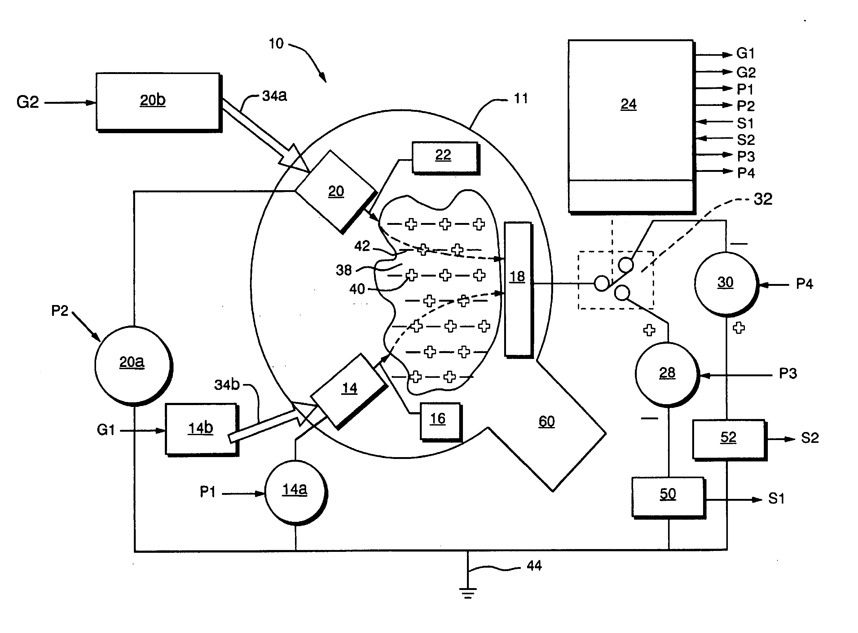
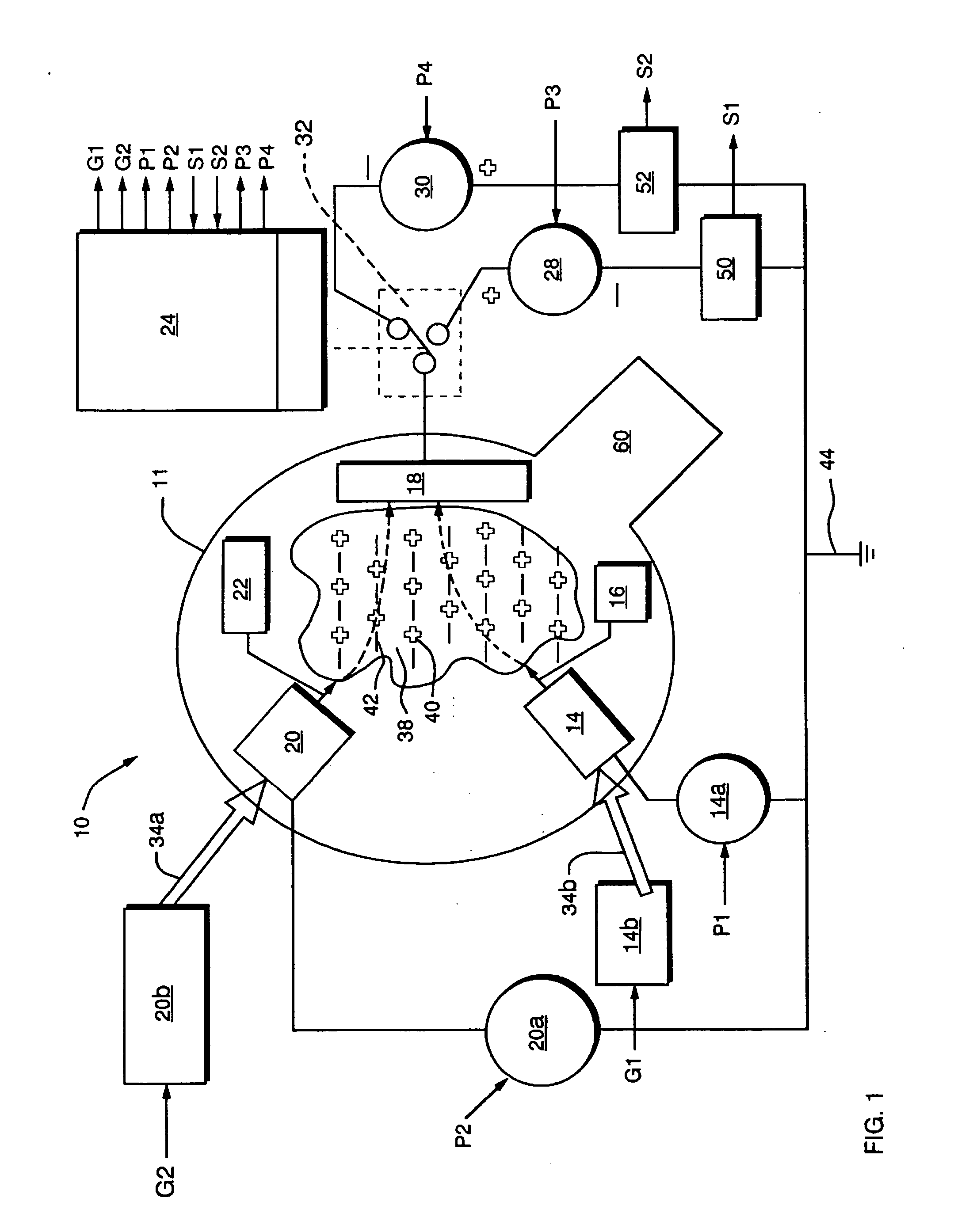
There is shown in FIG. 1, a system 10 for performing sputter etching for removal of material from substrate 18. System 10 comprises an ion source 14 that generates an ion current 16. The ion current 16 is directed primarily at substrate 18. System 10 further comprises an electron source 20 that generates an electron current 22. The electron current 22 is directed at the substrate 18. The ion source 14, the electron source 20 and the substrate 18 are disposed in a chamber 11. A vacuum pump 13 reduces the pressure within the chamber 11. The pressure within the chamber 11 during operation is about 10−3 to 10−5 torr.

Exemplary ion sources 14 useful for implementing the present invention include end-Hall or closed drift Hall ion sources such as the Mark II™ source of Commonwealth Scientific Corp / Veeco Instruments and the EH-1000 source of Kaufman & Robinson, Inc. Exemplary electron sources 20 useful for implementing the present invention include hollow cathode electron sources such Com...


PUM

PropertyMeasurementUnit
electrode voltagesaaaaaaaaaa
DC voltageaaaaaaaaaa

Abstract

A system and method for performing sputter etching includes an ion source that generates an ion current that is directed at a substrate and an electron source that generates an electron current directed at the substrate. Biasing circuitry biases the substrate with an a-symmetric bi-polar DC voltage pulse signal. The biasing circuitry is formed from a positive voltage source with respect to ground, a negative voltage source with respect to ground and a high frequency switch. At least one current sensor, coupled to the biasing circuitry, monitors a positive current and a negative current from the substrate during one or more cycles of the a-symmetric bi-polar DC voltage pulse signal. A control system, coupled to the at least one current sensor, varies the ion current independently from the electron current. The ion and electron sources create a continuous plasma that is proximate the substrate and the biasing circuitry causes the substrate to alternatively attract ions and electrons from the plasma. The ions attracted from the plasma sputter etch the substrate. The electrons attracted from the plasma neutralize accumulated charge on the substrate.

Description

FIELD OF INVENTION The present invention is directed generally to novel systems and methods for performing sputter etching for material removal. More particularly, the present invention is directed to improved systems and methods for downstream plasma etching. BACKGROUND OF THE INVENTION Conventional plasma sputter etching methods include DC (direct-current) diode sputtering, capacitively-coupled radio-frequency (RF) sputtering and downstream plasma sputtering. The first two methods require relatively high gas pressure (1 to 50 mTorr) and are unable to sustain a plasma discharge at low electrode voltages (below ˜300 volts). These characteristics limit the control of ion energies at the etched surface, particularly in the low energy regime, which may be important for low-damage etching of sensitive structures. The downstream plasma etching method uses a remote plasma source or plasma generator that, depending upon the characteristics of the plasma source, may allow lower pressure o...

Claims


Application Information

Patent Timeline
Patent Type & Authority Applications(United States)
IPC IPC(8): C23C14/46C23C14/54H01J37/317H01J37/34
CPCC23C14/46C23C14/54H01J37/34H01J37/3233H01J37/3178
Inventor BALDWIN, DAVID ALANHYLTON, TODD LANIER
Owner 4WAVE
Why Eureka
Try Eureka