Semiconductor device and method of manufacturing therefor

a semiconductor and semiconductor technology, applied in the field of semiconductor devices, can solve the problems of large off current of crystalline tft, degradation phenomenon, and large off current, and achieve the effect of increasing the reliability of a semiconductor device and increasing the aperture ratio

Inactive Publication Date: 2005-01-13
SEMICON ENERGY LAB CO LTD
View PDF48 Cites 41 Cited by
  • Summary
  • Abstract
  • Description
  • Claims
  • Application Information

AI Technical Summary

Benefits of technology

[0015] The present invention is a technique for solving this type of problem, and an object of the invention is to realize a crystalline TFT in which reliability equivalent to, or greater than, that of a MOS transistor can be obtained. Another object of the present invention is to increase the reliability of a semiconductor device having a large

Problems solved by technology

However, there is a problem in that the off current of the crystalline TFT is liable to become large.
The cause of this is the hot carrier effect, and it is thought that the hot carrier generated by the high electric field in the vicinity of the drain causes the degradation phenomenon.
However, the required characteristics are not necessarily the same for a TFT as a pixel section switching element and a driver circuit TFT such as a shift register circuit or a buffer circuit.
Furthermore, compared with an ordinary LDD structure, there is a problem with the GOLD structure in that the OFF current becomes large.
In order to prevent an increase in the OFF current, it is possible to make a multi-gate structure in which a plural number of gates are formed

Method used


Image

  • Semiconductor device and method of manufacturing therefor
  • Semiconductor device and method of manufacturing therefor
  • Semiconductor device and method of manufacturing therefor

Examples


embodiment mode 1

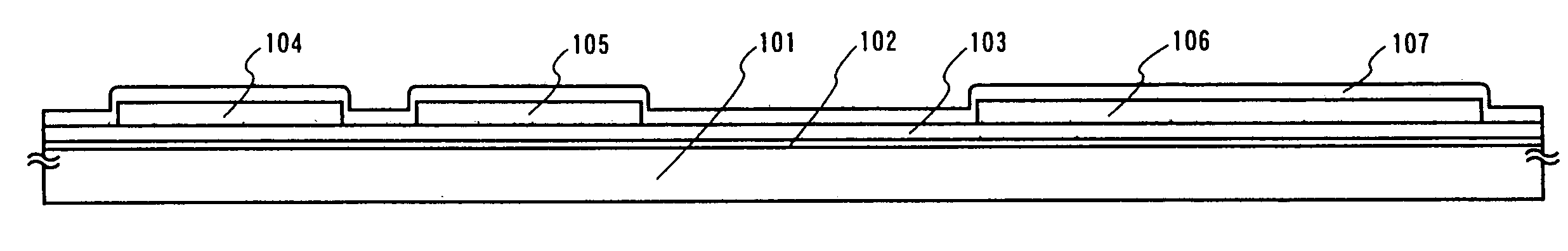
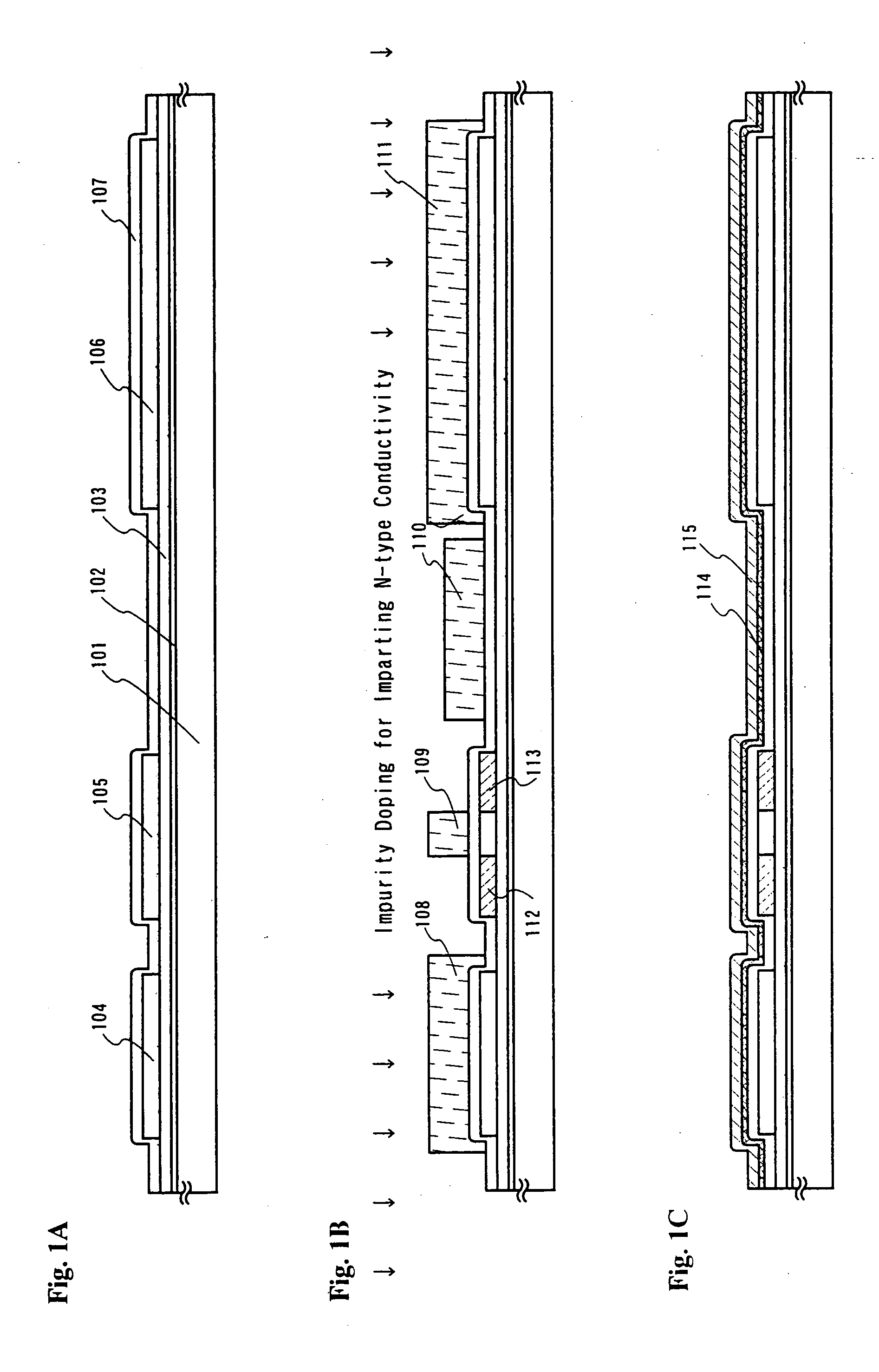
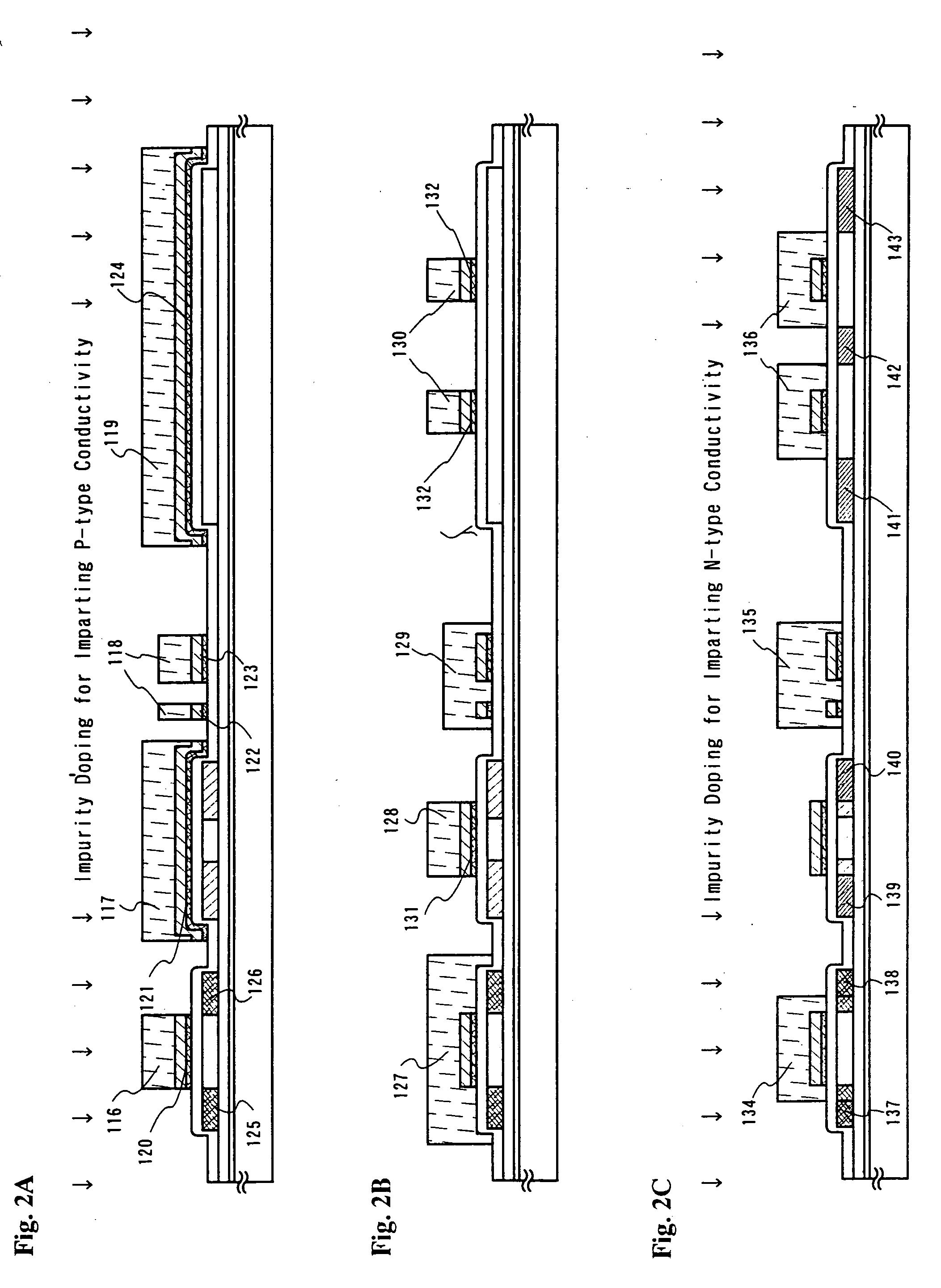
[0047] The embodiment modes of the present invention are explained using FIGS. 1A to 3C. A method of manufacturing a pixel section and driver circuit TFTs formed in the periphery at the same time is explained.

[0048] -Process of Forming Island Shape Semiconductor Layers and Gate Insulating Films

[0049] It is preferable to use a non-alkaline glass substrate or a quartz substrate as a substrate 101 in FIG. 1A. In addition, a silicon substrate, and a metallic substrate on which an insulating film is formed on its surface may also be used. A base film 102 is then formed from a silicon oxide film, a silicon nitride film, or an oxidized silicon nitride film by plasma CVD or sputtering to a thickness of between 100 and 400 nm on the surface of the substrate 101 on which the TFTs will be formed. For example, a two layer structure may be used as the base film 102, with a silicon nitride film 102 from 25 to 100 nm, a thickness of 50 nm is used here, and a silicon oxide film 103 from 50 to 300...

embodiment mode 2

[0077] Another structure for the storage capacitor connected to the n-channel TFT of the pixel section of the active matrix substrate is explained. FIG. 4 shows a cross sectional structure diagram of the pixel section of the active matrix substrate manufactured similar to that of embodiment mode 1.

[0078] Base films 402 and 403 are formed on a substrate 401, and a first impurity region and a fourth impurity region are formed in an island shape semiconductor layer 404. A gate electrode 406 is formed on a gate insulating film 405, and a source wiring 408 and a drain wiring 409 are formed on a first interlayer insulating film 407. A light shielding film 412 and a pixel electrode 418 are then formed over a passivation film 410 and a second interlayer insulating film 411.

[0079] A storage capacitor 421 connected to an n-channel TFT 420 is formed from the light shielding film 412 formed on the second interlayer insulating film 411, a dielectric film 413 formed on that, and the pixel elect...

embodiment mode 3

[0080] Another structure of a storage capacitor connected to the n-channel TFT of the pixel section is shown in FIGS. 5A to 5C. FIG. 5A is a pixel section n-channel TFT manufactured similar to that of embodiment mode 1. Base films 502 and 503 are formed on a substrate 501, and a first impurity region and a fourth impurity region are formed in an island shape semiconductor layer 504. A gate electrode 506 is formed on a gate insulating film 505, and a source wiring 508 and a drain wiring 509 are formed on a first interlayer insulating film 507. In addition, a light shielding film 512 and a spacer 513 formed by an organic resin are formed over a passivation film 510 and a second interlayer insulating film. A dielectric film 514 is next formed on the surface of the light shielding film by anodic oxidation, as shown in FIG. 5B. A pixel electrode 518 is connected to the drain wiring 509 by an opening 515 formed in the passivation film 510, by an opening 516 formed in a second interlayer i...


PUM


Abstract

In an active matrix type liquid crystal display device, in which functional circuits such as a shift register circuit and a buffer circuit are incorporated on the same substrate, an optimal TFT structure is provided along with the aperture ratio of a pixel matrix circuit is increased. There is a structure in which an n-channel TFT, with a third impurity region which overlaps a gate electrode, is formed in a buffer circuit, etc., and an n-channel TFT, in which a fourth impurity region which does not overlap the gate electrode, is formed in a pixel matrix circuit. A storage capacitor formed in the pixel matrix circuit is formed by a light shielding film, a dielectric film formed on the light shielding film, and a pixel electrode. Al is especially used in the light shielding film, and the dielectric film is formed anodic oxidation process, using an Al oxide film.

Description

BACKGROUND OF THE INVENTION [0001] 1. Field of the Invention [0002] The present invention relates to a semiconductor device having a circuit comprising a thin film transistor on a substrate having an insulating surface, and a manufacturing method therefor. In particular, the present invention can ideally be used in electro-optical devices, typically liquid crystal display devices in which an active matrix circuit and a driver circuit formed on its periphery, are formed on the same substrate, and in electronic equipment loaded with an electro-optical device. Note that semiconductor device, in this specification, indicates general devices that function by using semiconductor characteristics. Note also that the above stated electro-optical devices, and electronic equipment loaded with the electro-optical device, are included in that category. [0003] 2. Description of the Related Art [0004] The development of semiconductor devices having large surface area integrated circuits formed by ...

Claims


Application Information

Patent Timeline
IPC IPC(8): G02F1/1362H01L21/77H01L21/84H01L27/12H01L29/786
CPCG02F1/13454H01L27/1214H01L29/78621H01L29/78627H01L29/78645H01L29/78675H01L27/12G02F1/136209G02F1/136213H01L27/1255H01L29/78651G02F1/136286G02F1/1368H01L27/124
Inventor YAMAZAKI, SHUNPEIMURAKAMI, SATOSHIKOYAMA, JUNTANAKA, YUKIOKITAKADO, HIDEHITO
Owner SEMICON ENERGY LAB CO LTD
Why Eureka
Try Eureka