

Production method for soi wafer
a production method and technology of soi wafer, applied in the direction of basic electric elements, electrical apparatus, semiconductor devices, etc., can solve the problems of reducing the production yield, high density of crystal defects, and the aforementioned methods suffer from the drawbacks described, so as to reduce the surface roughness suppress the crystal defect and the soi layer surface roughness, and improve the film thickness distribution of the soi layer
- Summary
- Abstract
- Description
- Claims
- Application Information
AI Technical Summary
Benefits of technology
Problems solved by technology
Method used
Image

Examples
first embodiment
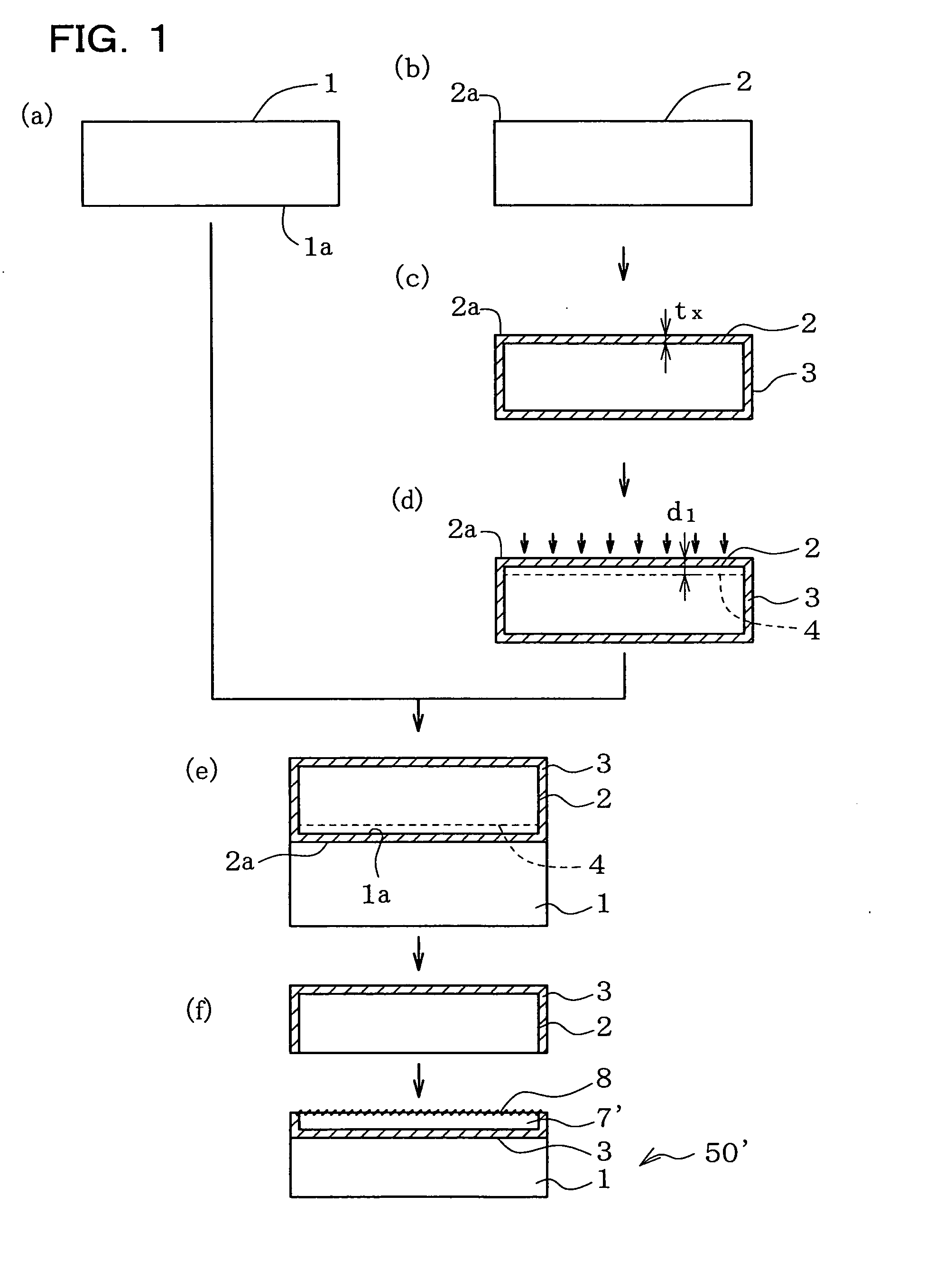
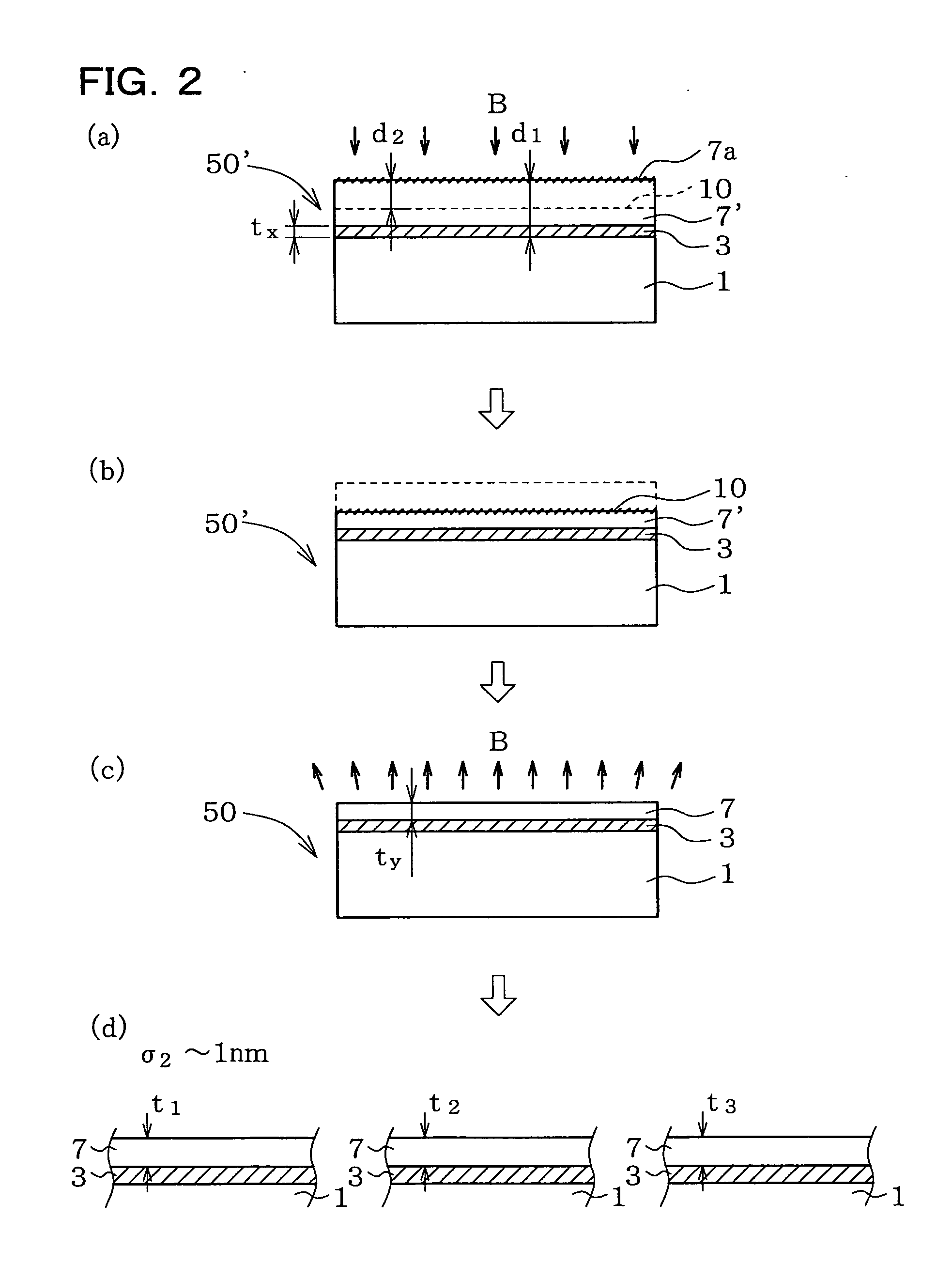
FIG. 1 is a drawing schematically explaining the method of fabricating an SOI wafer of this invention based on an exemplary case of using Smart Cut Process. First, a base wafer 1 (silicon single crystal wafer) as a first substrate shown in process step (a) and a bond wafer 2 (silicon single crystal wafer) as a second substrate shown in process step (b) are obtained. In the embodiment shown in FIG. 1, as shown in process step (c), a silicon oxide film 3 is formed as an insulating film on the surface of the bond wafer 2. The silicon oxide film 3 can typically be formed by thermal oxidation such as wet oxidation, where it is of course allowable to adopt other methods such as CVD (Chemical Vapor Deposition). Thickness of the silicon oxide film tx is typically set to a known value ranging from 50 nm to 2 μm or around. It is also allowable to use, in place of the silicon oxide film 2, an insulating film such as silicon nitride film or silicon oxynitride film.
Next, as shown in process st...
second embodiment
FIG. 7 explains a basic embodiment of the method of fabricating an SOI wafer according to the second embodiment of this invention. First, a base wafer 107 as a first silicon single crystal substrate shown in process step (b) and a bond wafer 101 as a second silicon single crystal substrate shown in process step (a) are obtained. As shown in process step (a), the bond wafer 101 herein has, formed on a first main surface J side thereof, a silicon oxide film 102 as an insulating film. The silicon oxide film 102 can typically be formed by thermal oxidation such as wet oxidation, where it is of course allowable to adopt other methods such as CVD (Chemical Vapor Deposition). Thickness of the silicon oxide film 102 ta is typically set to 50 nm to 2 μm or around, considering that it is used as an insulating layer typically in MOS-FET or the like.
Then, as shown in process step (a), the first main surface J of the bond wafer 1, or the main surface J on which the silicon oxide film 102 is fo...
PUM
 Abstract
Description
Claims
Application Information