Method and apparatus for forming fluoride thin film

a technology of fluoride thin film and forming method, which is applied in the direction of electrolysis components, vacuum evaporation coatings, coatings, etc., can solve the problems of poor adhesion between the film and the substrate, insufficient strength of the obtained film, and difficult development of automatic production machines

Inactive Publication Date: 2005-02-03
CANON KK
View PDF11 Cites 12 Cited by
  • Summary
  • Abstract
  • Description
  • Claims
  • Application Information

AI Technical Summary

Problems solved by technology

Although the vapor deposition method is a film-forming method that can form films rapidly on a large-area substrate using a simple-structure apparatus and is excellent in productivity, the method has posed the problems that highly accurate control of the film thickness and development of an automatic production machine are difficult, and that if a film is formed in a state of a low substrate temperature, the obtained film will have an insufficient strength and is liable to be scratched, and that the adhesion between the film and the substrate is poor.
However, fluorides such as MgF2 and AlF3, which are important materials for thin films having such a low refractive index as 1.45 or less and having a large influence on the optical performance of multilayer optical thin films, have a problem that low-absorption thin films cannot easily be formed.
However, even if a fluorine-based gas is introduced to complement fluorine atoms, as compared with the quantity of metal atoms that are sputtered from the target and impinge on the substrate, active fluorine atoms formed by dissociation in a plasma in the vicinity of the target and fluorine-containing gas molecules are consumed to fluorinate the target and the metallic atoms deposited on a portion other than the substrate in the vicinity of the target and only a small quantity thereof reaches the surface of the substrate, resulting in shortage of fluorine in the film on the substrate.
Moreover, if sputtering is performed in a state in which fluorine is adsorbed to the surface of the target, and the surface of the target is fluorinated, there are posed the problems of occurrence of abnormal discharge or significant dust generation.
Therefore, when the above-mentioned sputtering method is used, since the quantity of fluorine atoms that impinge on the substrate is insufficient, and the bonding state is disturbed, only MgF2 thin films with a large absorption can be formed.

Method used


Image

  • Method and apparatus for forming fluoride thin film
  • Method and apparatus for forming fluoride thin film
  • Method and apparatus for forming fluoride thin film

Examples


example 1

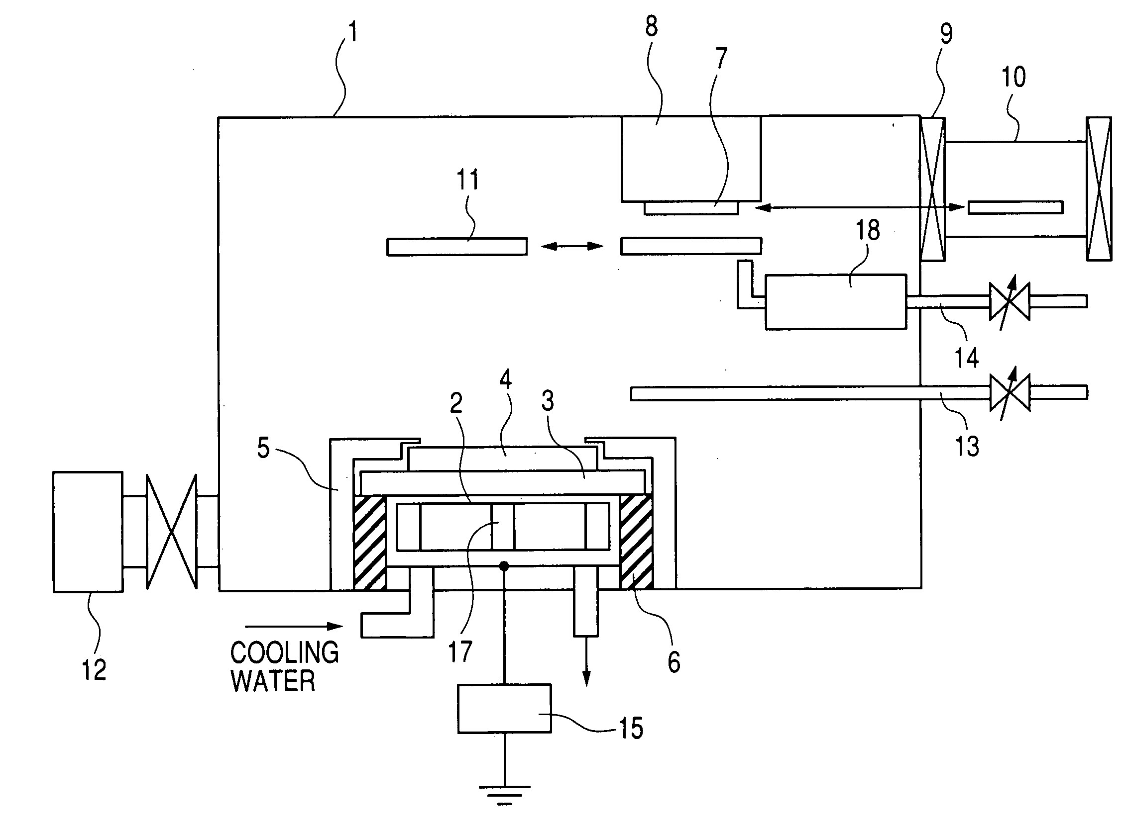
FIG. 1 is a schematic sectional view of a DC magnetron sputtering apparatus according to Example 1 of the present invention. As shown in FIG. 1, the sputtering apparatus is equipped with a vacuum vessel 1 that can maintain the inside in a substantially vacuum state. On the bottom center of the vacuum vessel 1, a cathode 2 that houses a magnet therein and can be cooled by water is provided. A backing plate 3 is placed on the upper surface of the cathode electrode 2, and a high-purity Mg metal target 4 is fixed on the upper surface of the packing plate 3. The material for the target may include various metals, and oxygen-added metals or fluorine-added metals can be used as long as the electrical resistance is low. An anode electrode 5 is fixed to the vacuum vessel 1 with a predetermined gap to the target 4. Incidentally, an insulator 6 is disposed between the anode electrode 5 and the backing plate 3.

On the upper surface of the vacuum vessel 1, an article to be processed 7 is movabl...

example 2

In this Example, a fluoride thin film was formed on a substrate by following the same procedure as in Example 1 with the exception that an La metal target was used in place of the Mg metal target and SF6 gas was used in place of F2 gas.

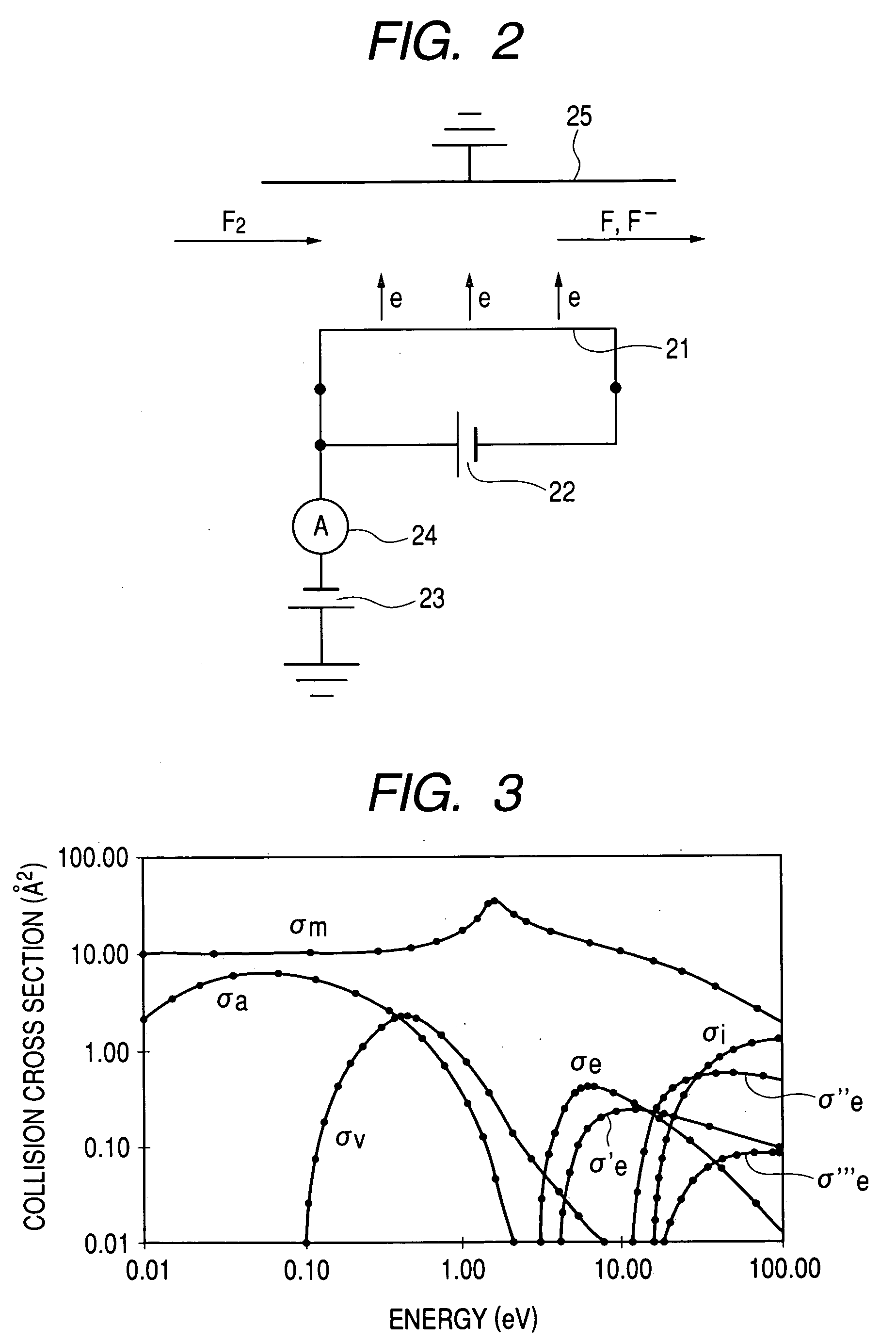
FIG. 4 shows a graph of the electron collision cross section of SF6 gas. As is seen from the graph of FIG. 4, also in the case of SF6 gas, although the dissociative electron attachment cross section is large when the electron energy is 1 eV or less, there is a peak of the dissociative electron attachment cross section at around 5 eV. Therefore, in this Example, 5 V was applied to the accelerating power source so as to accelerate thermal electrons emitted from the filament in the radical generator to 5 eV. By elevating the accelerating voltage, the current of the thermal electrons could be increased, thereby generating a sufficient quantity of active fluorine.

The obtained LaF3 thin film exhibited no absorption throughout a region ranging from the v...


PUM

PropertyMeasurementUnit
refractive indexaaaaaaaaaa
ionization energyaaaaaaaaaa
antireflectiveaaaaaaaaaa

Abstract

There are provided a method and an apparatus for forming a fluoride thin film having a desired refractive index and no absorption throughout a range including the ultraviolet region and the visible region, using a sputtering method. The method of forming a fluoride thin film according to the present invention is a method of forming a metal fluoride thin film on a substrate by performing reactive sputtering with a gas comprising fluorine by use of a metal target, which comprises irradiating a gas comprising fluorine with electrons having an energy less than the ionization energy of the gas comprising fluorine to activate the gas and introducing the activated gas into a reaction apace, thereby performing sputtering.

Description

This application claims priority from Japanese Patent Application No. 2003-284692 filed on Aug. 1, 2003, which is hereby incorporated by reference herein. BACKGROUND OF THE INVENTION 1. Field of the Invention The present invention relates to an optical thin film, such as an antireflective film and a dielectric multilayer mirror, used in optical components for visible and ultraviolet regions, and a method for manufacturing the same. 2. Related Background Art Heretofore, when an optical thin film such as an antireflective film or a mirror is formed, a vacuum vapor deposition method has been mainly used in which a film-forming material is heated by means of an electron beam or the like in a vacuum to be deposited on a substrate. In general, the antireflective film, mirror or the like is composed of either one of a material having a low refractive index such as magnesium fluoride (MgF2), and a material having a high refractive index such as zirconium oxide (ZrO2), tantalum oxide (T...

Claims


Application Information

Patent Timeline
Patent Type & Authority Applications(United States)
IPC IPC(8): C23C14/00G02B1/11C23C14/06C23C14/32C23C14/34
CPCC23C14/0047C23C14/0694C23C14/0057
Inventor TAKAKI, SATOSHI
Owner CANON KK
Why Eureka
Try Eureka