Circuit and method for suppression of electromagnetic coupling and switching noise in multilayer printed circuit boards

a technology of electromagnetic coupling and switching noise, which is applied in the incorporation of printed capacitors, waveguide type devices, line-transmission details, etc., can solve the problems of increasing material and manufacturing costs with increasing concomitantly, and achieve the effect of eliminating power plane resonance and suppressing digital nois

Inactive Publication Date: 2005-02-10
WEMTEC
View PDF47 Cites 152 Cited by
  • Summary
  • Abstract
  • Description
  • Claims
  • Application Information

AI Technical Summary

Benefits of technology

By way of introduction only, the present embodiments provide a two-dimensional, periodic, metallic structure, which acts as a distributed microwave bandstop filter integrated into a parallel-plate waveguide. These embodiments can be used as an electromagnetic interference (EMI) filter to suppress digital noise on power planes, as well as to eliminate power plane resonances. Hence, they may be used for EMI and EMC (electromagnetic compatibility) purposes in printed circuit boards.

Problems solved by technology

The new structure, when used as part of a printed circuit board design, permits elimination of many of the higher frequency surface-mounted bypass capacitors used in conventional PCB designs, along with the concomitant increased material and manufacturing costs.

Method used


Image

  • Circuit and method for suppression of electromagnetic coupling and switching noise in multilayer printed circuit boards
  • Circuit and method for suppression of electromagnetic coupling and switching noise in multilayer printed circuit boards
  • Circuit and method for suppression of electromagnetic coupling and switching noise in multilayer printed circuit boards

Examples


first embodiment

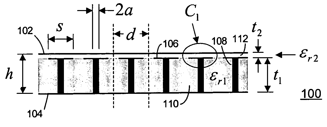
Referring now to the drawing, FIG. 1 and FIG. 2 illustrate a parallel plate wave guide (PPW) 100 containing a transverse electromagnetic (TEM) mode suppression circuit. FIG. 1 is a perspective view of the PPW 100 and FIG. 2 is a cross-sectional view of the PPW 100. Coordinate axes establish the x, y and z directions as used herein.

As shown in FIGS. 1 and 2, the PPW 100 includes an upper conductive plate 102, a lower conductive plate 104, an array of conductive coplanar patches 106 located a distance t2 from the upper plate 102, an array of conductive rods or vias 108 of length t1 and radius a that connect the lower plate 104 to the center of each patch 106, a first dielectric layer 110 and a second dielectric layer 112. The patches 106 are illustrated to be squares of side length s in FIG. 1, but other shapes such as rectangular, hexagonal, triangular, circular, etc. can be used. The patch realizes a parallel-plate capacitance between the end of the rod 108 below it and the upper p...

example

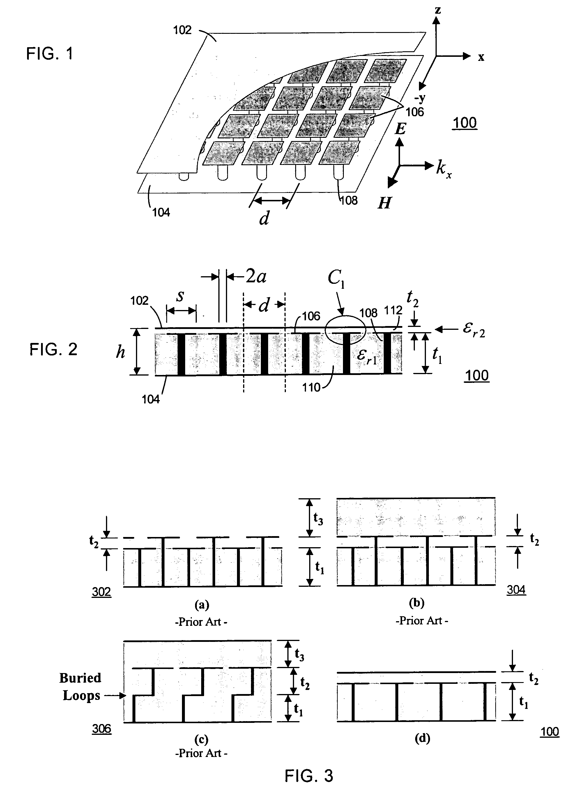
(d) of FIG. 3 shows the PPW 100 embodiment of FIGS. 1 and 2. Here, the upper layer of patches of the high-impedance surface of example (a) has been replaced with a solid metal plane, the upper plate of the PPW 100. The total height of this structure can be less than 1 mm and the PPW 100 can still achieve a bandwidth in excess of 6:1 for the fundamental stopband using only conventional printed circuit board (PCB) materials and processes. Furthermore, the thickness t2 is typically less than 0.1 mm. This will be described in greater detail below.

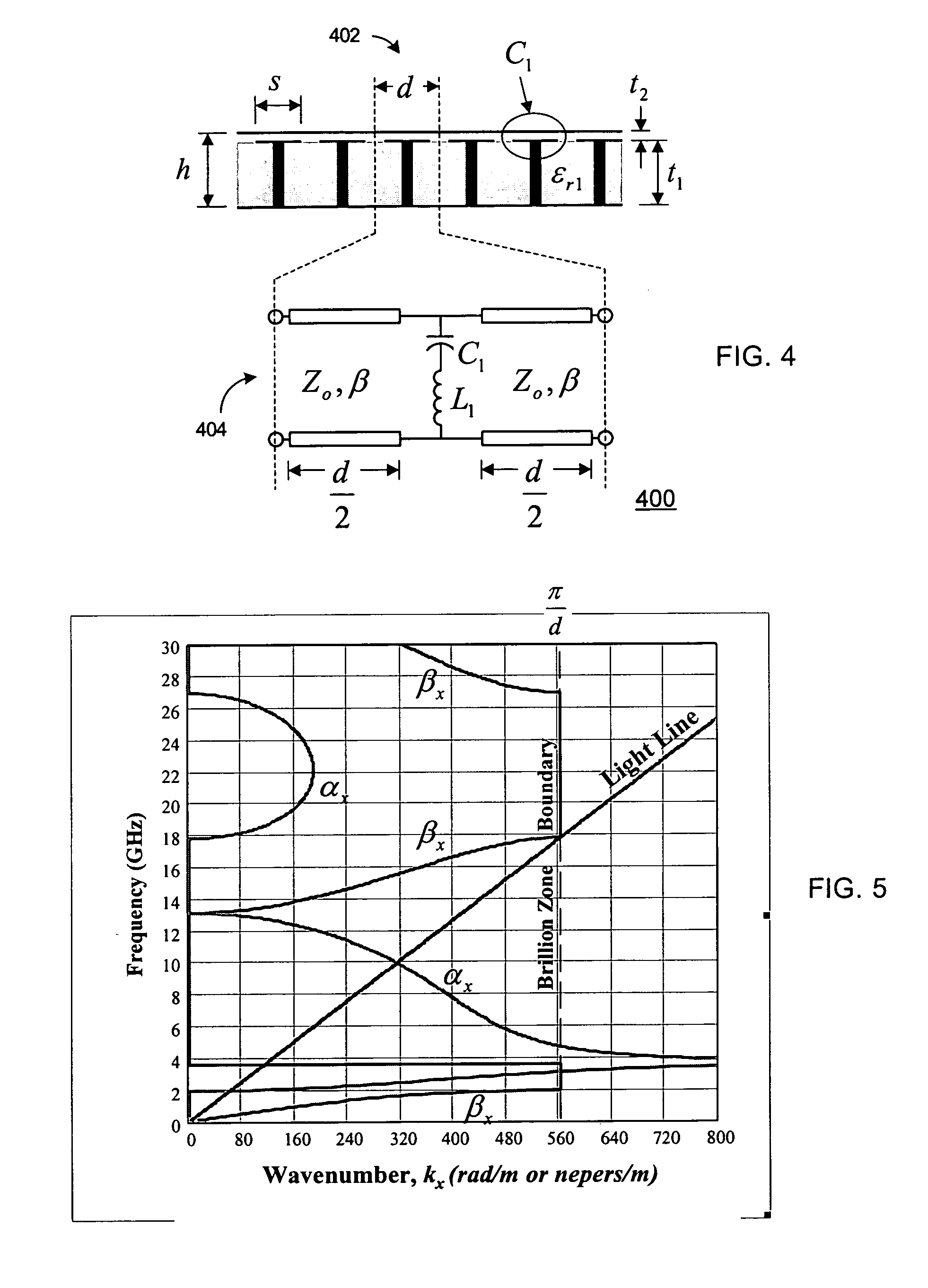
FIG. 4 illustrates a transmission line model 400 for the embodiment of FIGS. 1 and 2. The stopband properties of the present embodiments may be understood through a circuit analysis of only one unit cell 402. A quasi-TEM mode on the empty PPW (without patches or vias) can be modeled as a simple transmission line 404 whose characteristic impedance and phase constant are given by  ⁢Zo=ηoɛr,eff⁢hd(1)β=ωc⁢ɛr,eff(2)

where ηo is the wave impedance o...

fourth embodiment

Yet another embodiment involves adding a spiral inductor in series with each via, as shown in FIGS. 16 and 17. The purpose of this added inductance is to reduce flower. FIG. 16 and FIG. 17 illustrate a parallel plate waveguide (PPW) 1600. The PPW 1600 includes an upper conductive plate and a lower conductive plate (not shown in FIG. 16). The PPW 1600 includes an array of conductive coplanar patches 1606 located a distance t2 from the upper plate, an array of conductive rods or vias 1608 of length t1 and radius a that connect the lower plate to the center of each patch 1606, a first dielectric layer 1610 and a second dielectric layer 1612. The PPW 1600 further includes a spiral inductor 1612 associated with each respective patch 1606 and via 1608.

In the embodiment of FIGS. 16 and 17, the inductors 1614 and patches are coplanar and are etched as part of the same metal layer. The coplanar spiral inductor 1614 is formed within the perimeter of the patch 1606. The merit of an embedded s...


PUM


Abstract

Apparatus for suppressing noise and electromagnetic coupling in the printed circuit board of an electronic device includes an upper conductive plate and an array of conductive coplanar patches positioned a distance t2 from the upper conductive plate. The distance t2 is chosen to optimize capacitance between the conductive coplanar patches and the upper conductive plate for suppression of noise or electromagnetic coupling. The apparatus further includes a lower conductive plate a distance t1 from the array of conductive coplanar patches and conductive rods extending from respective patches to the lower conductive plate.

Description

BACKGROUND This invention is related generally to reduction of noise induced in power planes due to switching of digital circuits. More particularly, the present invention is related to circuits and method for suppression of transverse electromagnetic modes in parallel plate waveguides. A common problem in electronic systems is switching noise induced in the power distribution system by switching of digital circuits of the system. Conventionally, such a system has one or more power planes designated, for example, +Vcc, and one or more ground planes. The potential difference between the power plane and the ground plane provides the DC operating voltage for the circuits of the system. If the system includes digital or other circuits with fast-switching outputs, noise can be induced in the power planes and even in the ground plane. The noise may have several sources, but generally is due to the high slew rate of the digital output and the non-zero inductance of the power plane. Espec...

Claims


Application Information

Patent Timeline
Patent Type & Authority Applications(United States)
IPC IPC(8): H01L23/58H01L23/62H01P1/16H04B3/04H05KH05K1/16
CPCH01P1/16H01P1/2005H05K2201/09663H05K2201/093H05K2201/09309H05K1/162
Inventor MCKINZIE, WILLIAM E. IIIROGERS, SHAWN D.
Owner WEMTEC
Why Eureka
Try Eureka