Dummy fill structures can be added to improve process uniformity. Adding metal dummy fill increases the pattern density since density is defined as the amount of metal divided by the total area within a given region. Conversely, adding oxide dummy removes sections of the
copper line and decreases the pattern density. The addition of fill can also alter other parameters such as linewidth and linespace. If dummy metal is inserted between two parallel lines, the linespace changes for both of those lines. Similarly, if oxide dummy is inserted within a wire, its effective linewidth is changed. By modifying the existing layout through the addition of dummy fill, physical parameters such as pattern density, linewidth, and linespace are changed. Since metal or oxide film thickness non-uniformity resulting from CMP is dependent on these physical parameters, the addition or removal of metal alters the physical characteristics of the designed layout. Therefore, the addition of metal or oxide fill based on process models can reduce the film thickness non-uniformity.
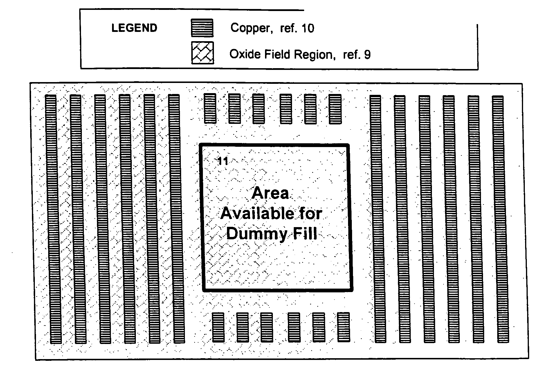
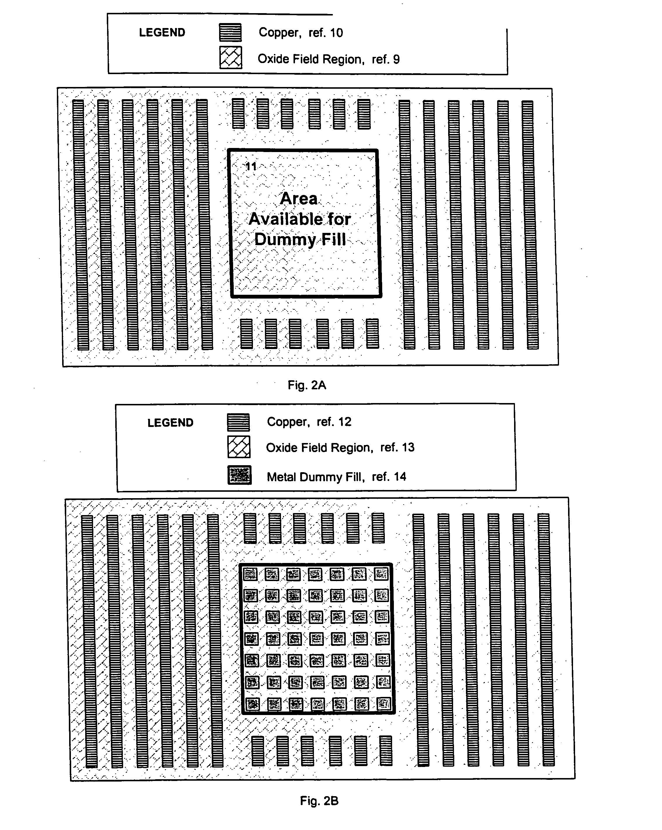
Dummy fill is a method of improving film thickness uniformity in integrated circuits through the addition or removal of existing structures. The following two figures illustrate two types of dummy fill, metal and oxide. FIG. 2 illustrates the use of metal dummy fill. FIG. 2A shows a series of metal lines, 10, in an oxide layer, 9, with a large oxide field region in the middle, 11, that is available for dummy fill. One goal of dummy fill is to achieve uniform pattern density everywhere so that deposition and
polishing process result in a planar film thickness. As such, this area would be selected as available for dummy fill. This region is particularly attractive in that it is of sufficient distance from electrically conducting lines and may minimize the
impact of dummy fill on
capacitance. In FIG. 2B, metal dummy fill, 14, has been placed in the oxide field area, 13, to raise the density of this region, while the metal dummy fill remains electrically isolated from the conducting regions, 12, around it.
FIG. 3 illustrates the addition of oxide dummy fill in a metal field. In FIG. 3A, metal field region, 15, has a large area, 16, available for oxide dummy fill. In FIG. 3B, oxide dummy fill (also referred to as metal slotting), 18, is added to the metal area, 17, raising the density of raised area of the region and subsequently improving the polishing uniformity (reducing the film thickness variation) of this region. The term “dummy fill area” is used to refer to the area where dummy fill is added and the term “dummy fill structures” is used to refer to the new objects that are embedded within that area.
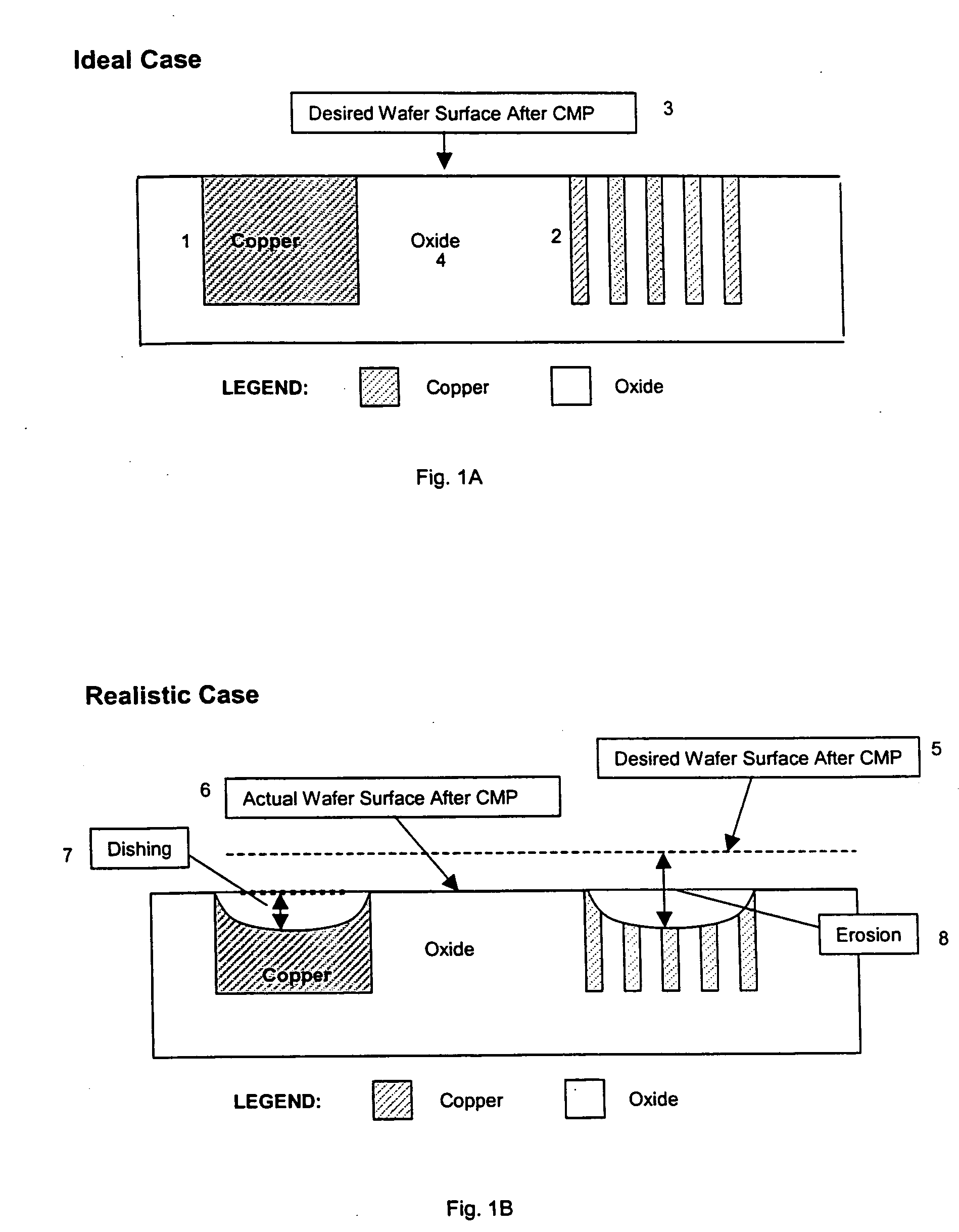
Once the
copper is deposited, it must be polished until all of the copper above the field regions is cleared. CMP is the leading method of copper removal and planarization in
semiconductor manufacturing processes. Differences in the structures and their surroundings result in variable polish rates across the chip. To guarantee that there are no shorts between interconnects, over-polishing is done until all the copper is cleared above the
field oxide. This results in metal thickness variation (see FIG. 4). Another application of dummy fill is to modify the interconnect structures and surrounding areas to reduce the variation. This can be done by adding metal dummy fill between the interconnect regions or removing metal from the existing interconnect. As such, the layout can be altered from its original design by adding additional features (metal dummy fill) or removing sections of existing features (slotting with oxide dummy fill). This improves process uniformity but can adversely affect the
electrical performance of the chip. Therefore, the goal is to fill the layout in a way that reduces the
process variation while preserving the original intended functions of the circuit.
Dummy fill objects are sized, and a dummy fill pattern of the objects is created for one or more interconnect levels of the
semiconductor design. The dummy fill information comprises dummy fill rules. The pattern includes oxide or metal dummy fill objects. The objects of the dummy fill pattern are placed to minimize full-chip film thickness variation. The objects of the dummy fill pattern are placed to minimize full-chip variation in electrical parameters. The electrical parameters comprise at least one of
sheet resistance, resistance,
capacitance,
crosstalk noise,
voltage drop, drive current loss, and effective
dielectric constant. The GDS files are modified to improve uniformity and electrical performance of the
semiconductor device. The process comprises a damascene process flow.
a web-based application comprised of web services is made available to a user on a network that enables the user to verify dummy fill information with respect to a semiconductor design and a fabrication process. The dummy fill placement strategy includes using dummy fill objects to improve a
structural integrity of low-K
dielectric features. The dummy fill placement strategy includes using dummy fill objects to maintain or improve an effective
dielectric constant of low-K dielectric features. The effective dielectric constant is maintained through all steps of a damascene process flow. The dummy fill placement strategy includes using dummy fill objects to facilitate integration of low-k dielectric materials into a damascene process flow.

