Methods and systems for implementing dummy fill for integrated circuits

a technology of integrated circuits and filling devices, applied in the direction of program control, total factory control, instruments, etc., can solve the problems of decreasing the pattern density, post-cmp oxide thickness variation, and subsequent manufacturability and process integration problems, so as to improve the uniformity and electrical performance of the semiconductor device, minimize the variation of full-chip electrical parameters, and minimize the effect of full-chip film thickness variation

Inactive Publication Date: 2010-07-13
CADENCE DESIGN SYST INC
View PDF110 Cites 16 Cited by
  • Summary
  • Abstract
  • Description
  • Claims
  • Application Information

AI Technical Summary

Benefits of technology

[0030]At an Internet server, a layout file for a semiconductor device is received from a client, dummy fill modifications to the layout file are generated at the server, and the dummy fill modified layout file is returned from the server to the client. At a server, a service is provided that enables a user to interactively configure a dummy fill application running on the server, and the user is enabled to generate dummy fill information using the dummy fill application. A service is made available to a user on a network that enables the user to verify dummy fill information with respect to a semiconductor design and a fabrication process. The dummy fill information that is verified includes at least one of a dummy fill pattern, a dummy fill strategy, or a dummy fill representation. The dummy fill information is verified with respect to a single interconnect level of the semiconductor design. The dummy fill information is verified with respect to multiple interconnect levels of the semiconductor design. Dummy fill objects are sized and a dummy fill pattern of the objects is created for one or more interconnect levels of the semiconductor design. The dummy fill information comprises dummy fill rules. The pattern includes oxide or metal dummy fill objects. The objects of the dummy fill pattern are placed to minimize full-chip film thickness variation. The objects of the dummy fill pattern are placed to minimize full-chip variation in electrical parameters. The electrical parameters comprise at least one of sheet resistance, resistance, capacitance, crosstalk noise, voltage drop, drive current loss, and effective dielectric constant. The GDS files are modified to improve uniformity and electrical performance of the semiconductor device. The process comprises damascene process flow. The network is an intranet, extranet or the internet.

Problems solved by technology

Surface non-uniformity often leads to subsequent manufacturability and process integration issues.
However, differences in the underlying metal pattern result in variation in the post CMP oxide thickness, even though a locally planar layer of oxide is achieved with CMP.
Conversely, adding oxide dummy removes sections of the copper line and decreases the pattern density.
Since metal or oxide film thickness non-uniformity resulting from CMP is dependent on these physical parameters, the addition or removal of metal alters the physical characteristics of the designed layout.
Therefore, the addition of metal or oxide fill based on process models can reduce the film thickness non-uniformity.
However, the addition of dummy structures may unintentionally affect the electrical properties and degrade chip performance.
The electrical performance of a circuit can be determined by the electrical characteristics of its interconnect, and the interconnect is often the limiting factor in high performance designs.
The addition of dummy fill can result in unwanted electrical effects.
Differences in the structures and their surroundings result in variable polish rates across the chip.
This improves process uniformity but can adversely affect the electrical performance of the chip.

Method used


Image

  • Methods and systems for implementing dummy fill for integrated circuits
  • Methods and systems for implementing dummy fill for integrated circuits
  • Methods and systems for implementing dummy fill for integrated circuits

Examples


Embodiment Construction

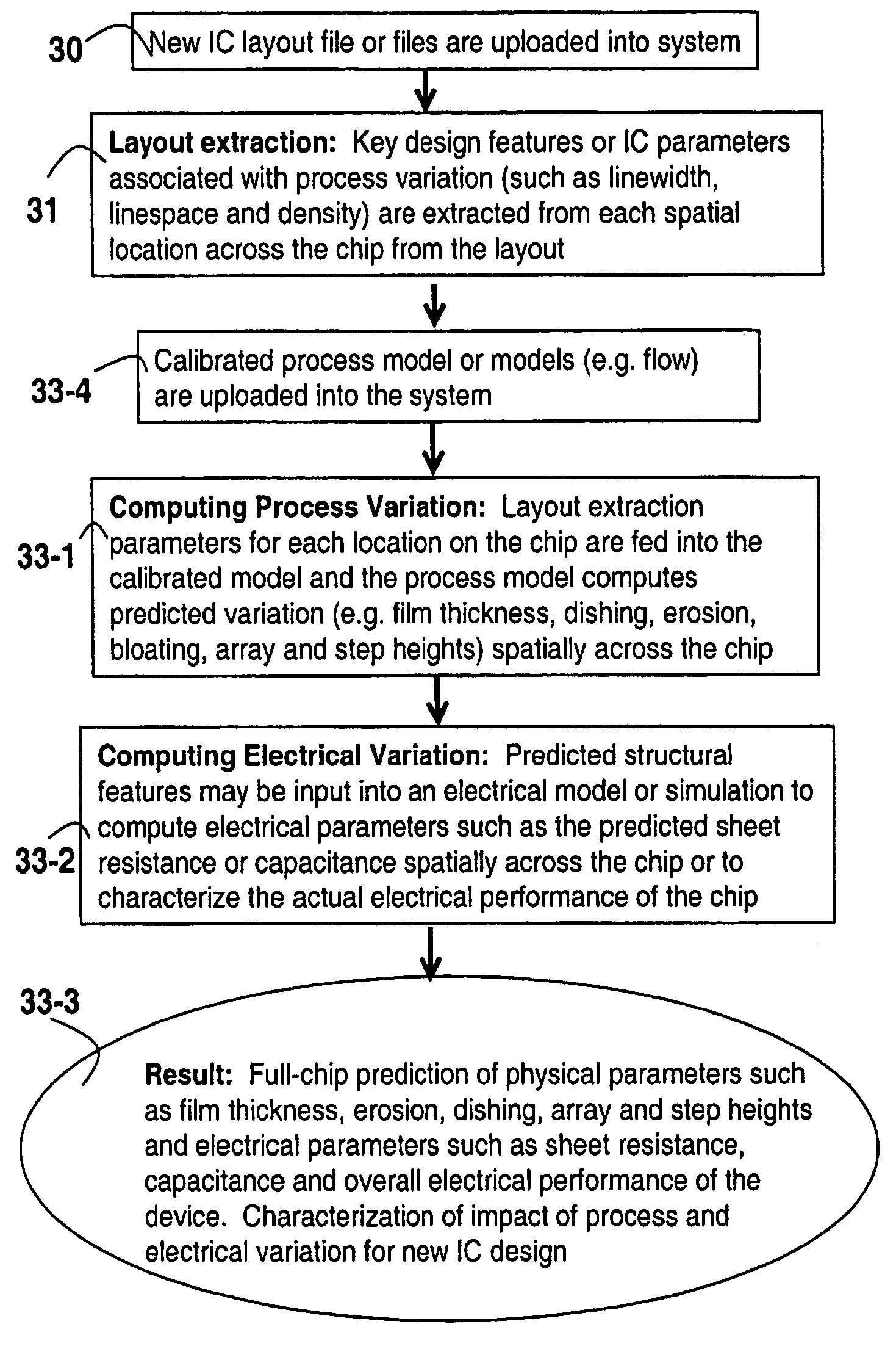
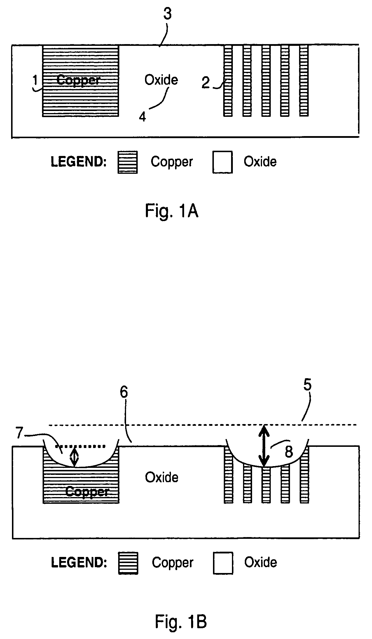
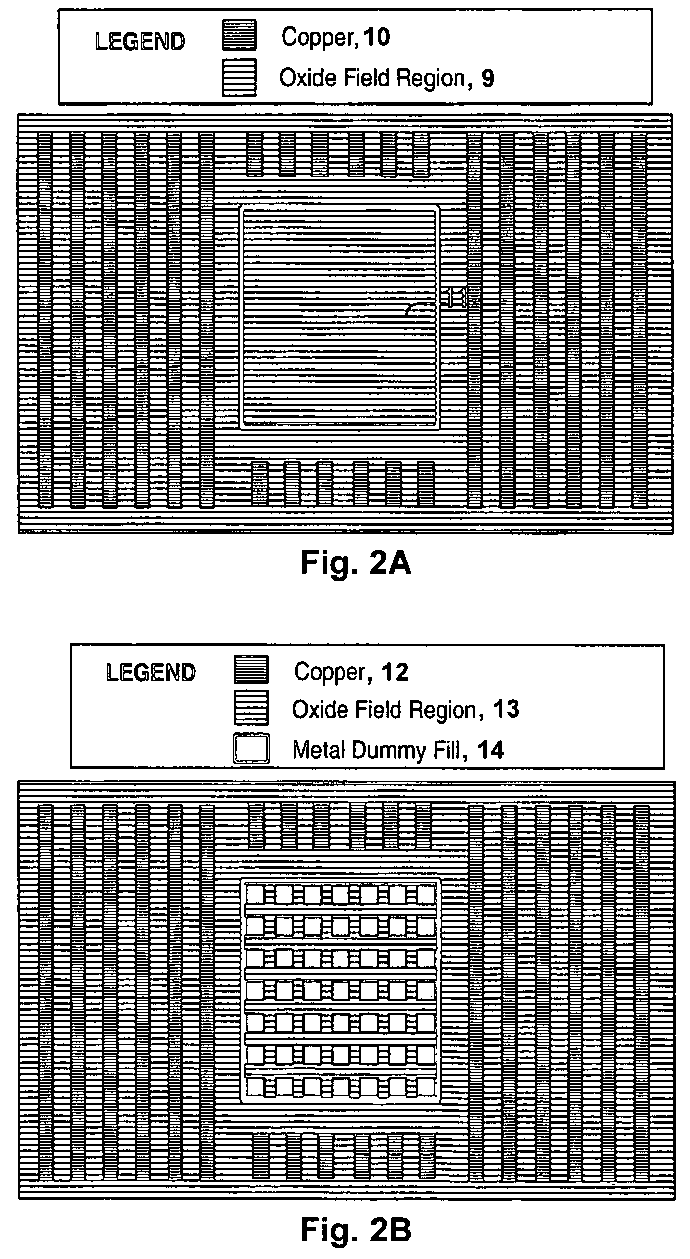
[0093]We describe a method of adding dummy fill to reduce process variations caused by dependencies in the electrochemical deposition and subsequent chemical mechanical polishing of interconnect features used in semiconductor devices. The variation in wafer quality (e.g. film thickness variation and surface topography variation such as dishing and erosion) and electrical parameters (resistance, capacitance, and noise) are modeled and simulated using semi-physical process models that may be calibrated to a particular process and tool for each step in a sequence of one or more steps within a process flow. Dummy fill structures are placed in the layout to improve thickness and surface topography uniformity of the manufactured wafer while maintaining the electrical parameters at the intended or designed values. The added structures are placed in such a way as to: modify the design layout parameters such as effective pattern density, maximum and minimum widths and spaces between structur...


PUM


Abstract

A method and system are described to reduce process variation as a result of the electrochemical deposition (ECD), also referred to as electrochemical plating (ECP), and chemical mechanical polishing (CMP) processing of films in integrated circuit manufacturing processes. The described methods use process variation and electrical impact to direct the insertion of dummy fill into an integrated circuit.

Description

CROSS-REFERENCE TO RELATED APPLICATIONS[0001]This application is a continuation of U.S. application Ser. No. 10 / 164,847, filed on Jun. 7, 2002, now U.S. Pat. No. 7,152,215 which is hereby incorporated by reference as if fully set forth herein.BACKGROUND[0002]This description relates to dummy fill for integrated circuits.[0003]In fabricating integrated circuits, interconnect film thickness uniformity, dishing, and erosion are dependent on variation in layout patterns (e.g. material density, linewidth and linespace). Surface non-uniformity often leads to subsequent manufacturability and process integration issues. These pattern dependencies may also affect device performance by introducing variation in capacitance and resistance depending on the location of a given structure on the device.[0004]Film thickness variation in chemical mechanical polishing (CMP) processes can be separated into various components: lot-to-lot, wafer-to-wafer, wafer-level, and die-level. Oxide thickness varia...

Claims


Application Information

Patent Timeline
Patent Type & Authority Patents(United States)
IPC IPC(8): G06F17/50H01L21/00H01L21/3105H01L21/321H01L21/768H01L23/522H01L27/02
CPCG06F17/5068H01L21/31053H01L21/3212H01L21/76819H01L21/7684H01L27/0207G06F2217/12H01L2924/0002H01L23/522H01L2924/00G06F30/39G06F2119/18Y02P90/02
Inventor SMITH, TABER H.MEHROTRA, VIKASWHITE, DAVID
Owner CADENCE DESIGN SYST INC
Why Eureka
Try Eureka