Insulating film and electronic device

a technology of electronic devices and films, applied in nanoinformatics, instruments, transistors, etc., can solve the problems of large gate leak current, power consumption is no longer pressed down from loss of standby power requirements, and the gate leak current has reached

Inactive Publication Date: 2005-02-24
KK TOSHIBA
View PDF1 Cites 40 Cited by
  • Summary
  • Abstract
  • Description
  • Claims
  • Application Information

AI Technical Summary

Problems solved by technology

However, as long as the SiO2 film is used, a gate leak current becomes large and power consumption is no longer pressed down from loss of standby power requirement.
For example, although MOSFET operates normally with SiO2 film of 8 angstroms (0.8 nm) of thickness, gate leak current has reached even 1 kA / cm2 and the problem in the field of power consumption is very big.
However, generally as for the materials with high permittivity, the band gap tends to become smaller.
Actually, in the gate insulating film using a substance with high permittivity like SrTiO3, since the band offset by the side of a conduction band becomes very small, it is difficult to stop the leak current by making the thickness quite thick.
The same problem exists in the case of MIM capacitors.
For example, in a Pt / SrTiO3 / Pt capacitor, since the leak current is very large, it is unutilizable.
However, from a view point of the miniaturization for high integration and the request of low power consumption, these laminated-type insulating films and the Ruddlesden-Popper type (Srn+1TinO3n+1) films were not sufficient to realize both higher permittivity and lower leak.
Furthermore, it is not taken into consideration about the shift of the optimum range at the time of introducing “distortion” into Si substrate.

Method used


Image

  • Insulating film and electronic device
  • Insulating film and electronic device
  • Insulating film and electronic device

Examples


examples

Referring to drawings, some embodiments of the present invention will now be described in more detail. The insulating film of the invention providing single quantum well structure or multi quantum well structure can be manufactured by the sputtering method, the laser ablation method, the chemistry gaseous phase growing-up method (CVD), etc. In the following examples, all of the thin film was grown up by the molecular beam epitaxy (MBE) method.

First, the molecular beam epitaxy equipment used in common will be explained. The vacuum vessel is exhausted by the cryopump. The ultimate vacuum was 10−6 Pa or less. A substrate holder is provided in a vacuum vessel and a substrate is installed in this substrate holder.

The substrate holder is heated at a heater. Two or more Knudsen cells are provided so that the substrate may be countered, and the cell shutter is provided in the opening of each Knudsen cell. In each Knudsen cell, the metal of each element selected from the group consistin...

second example

Next, MOSFET using the insulating film which has the single quantum well structure of SrO / SrTiO3 (it may omit following STO) / SrO as a second example of the present invention will be explained.

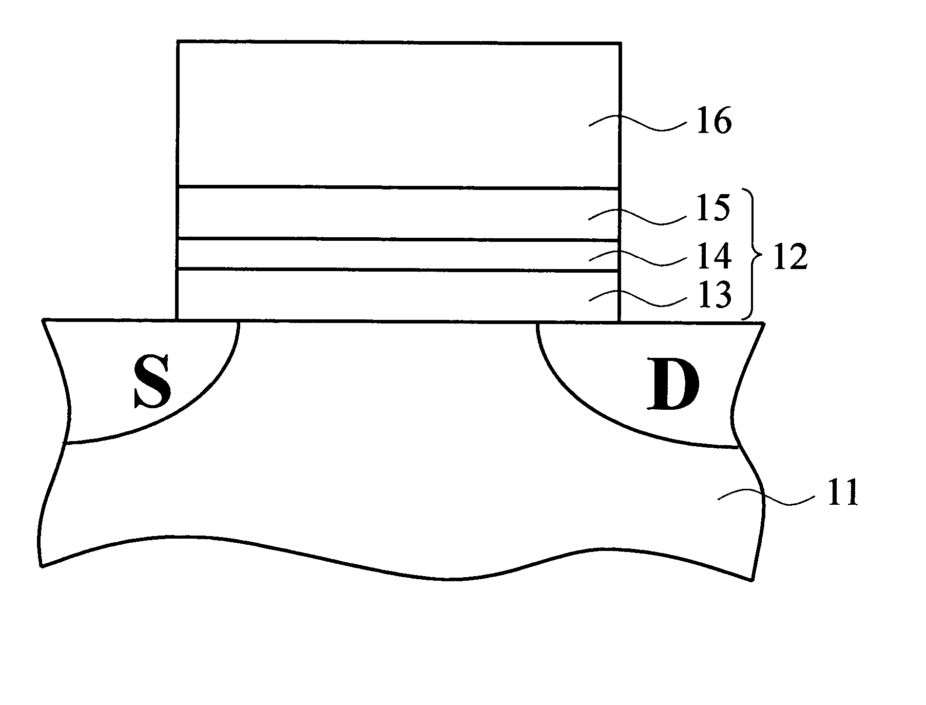
FIG. 11 is a sectional view of the gate insulating film of MOSFET of the second example of the present invention.

That is, in FET of this example, the source region S and the drain region D are formed in the surface of a silicon substrate 21, and the gate electrode 26 is provided through the gate insulating film 22 on the channel region which is formed between them. A gate insulating film has the single quantum well structure where the SrO barrier layer 23, the STO well layer 24, and the SrO barrier layer 25 were laminated.

This is explained in order of a manufacturing process. That is, first, the SrO (001) layer 23 was grown epitaxially on the Si substrate 21 whose major surface is (001). The thickness of the SrO layer 23 was made into about 5.2 angstroms. More specifically, first, only st...

third example

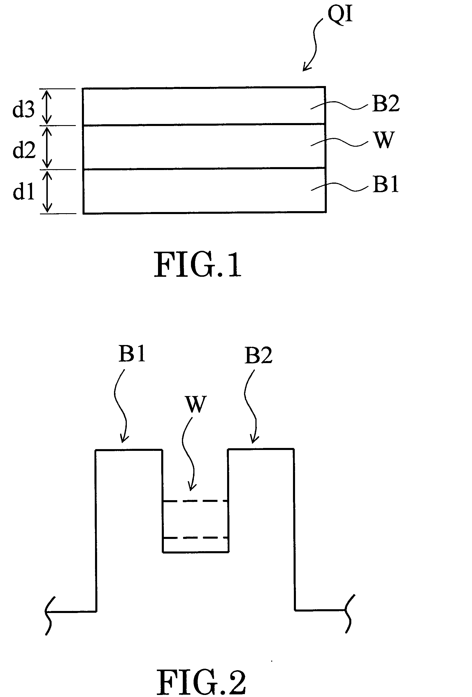
Next, MOSFET in which the insulating film which has double quantum well structure called SrO / STO / SrO / STO / SrO is provided will be explained as a third example of the invention.

FIG. 12 is a sectional view of the gate insulating film of MOSFET of the third example of the invention.

That is, in FET of this example, the source region S and the drain region D are formed in the surface of a silicon substrate 31, and the gate electrode 38 is provided through the gate insulating film 32 on the channel region which is formed between them. A gate insulating film has the double quantum well structure where the SrO barrier layer 33, the STO well layer 34, the SrO barrier layer 35, the STO well layer 36, and the SrO barrier layer 37 were laminated.

The manufacturing process of this is explained. That is, first, the SrO (001) layer 33 was grown epitaxially on the (001) Si substrate 31. The thickness of the SrO layer 33 was made into about 7.8 angstroms. More specifically, first, only strontium...


PUM


Abstract

An insulating film comprising: a first barrier layer;a well layer provided; and a second barrier layer is proposed. The first barrier layer consists of a material having a first bandgap and a first relative permittivity. The well layer is provided on the first barrier layer, and consists of a material having a second bandgap smaller than the first bandgap and having a second relative permittivity larger than first relative permittivity. Discrete energy levels are formed in the well layer by a quantum effect. The second barrier layer is provided on the well layer, and consists of a material having a third bandgap larger than the second bandgap and having a third relative permittivity smaller than second relative permittivity. Alternatively, an insulating film comprising: n (n being an integer larger than 2) layers of barrier layer consisting of a material having a bandgap larger than a first bandgap and having a relative permittivity smaller than a first relative permittivity; and (n−1) layers of well layers consisting of a material having a bandgap smaller than the first bandgap and having a relative permittivity larger than the first relative permittivity, discrete energy levels being formed in the well layer by a quantum effect, each of the barrier layers and each of the well layers being stacked by turns, and discrete energy levels being formed in each of the well layers by a quantum effect, is provided. Alternatively, an insulating film having a lattice mismatch within a range of plus-or-minus 1.5% to the substrate, and further having a high barrier and a large permittivity is provided.

Description

CROSS-REFERENCE TO RELATED APPLICATIONS This application is based upon and claims the benefit of priority from the prior Japanese Patent Application No. 2002-285034, filed on Sep. 30, 2002 and the prior Japanese Patent Application No. 2003-197808, filed on Jul. 16, 2003; the entire contents of which are incorporated herein by reference. BACKGROUND OF THE INVENTION The present invention relates to an insulating film and an electronic device, and more particularly, it relates to an insulating film suitably applied to an electric field effect type transistor and a metal-insulator-metal (MIM) capacitor, and to an electronic device having the insulating film. Furthermore, the present invention relates to electronic devices, such as a MOS field effect transistor which has the semiconductor substrate mainly constituted by Si (silicon) and a gate insulating film using the layered perovskite substance which is epitaxially grown directly on it. In order to carry out a miniaturization of UL...

Claims


Application Information

Patent Timeline
Patent Type & Authority Applications(United States)
IPC IPC(8): H01L27/04B82Y10/00B82Y40/00G11C11/401H01L21/02H01L21/28H01L21/314H01L21/316H01L21/336H01L21/822H01L29/12H01L29/15H01L29/51H01L29/78H01L29/786
CPCB82Y10/00H01L29/78H01L21/02156H01L21/02175H01L21/02178H01L21/02181H01L21/02189H01L21/02192H01L21/02197H01L21/022H01L21/02244H01L21/02255H01L21/02271H01L21/02293H01L21/02337H01L21/28185H01L21/28194H01L21/28291H01L21/3142H01L21/3147H01L21/3162H01L21/31641H01L21/31645H01L21/31691H01L28/56H01L29/122H01L29/152H01L29/513H01L29/517H01L29/518H01L21/02148H01L29/40111
Inventor SHIMIZU, TATSUOSATAKE, HIDEKI
Owner KK TOSHIBA
Why Eureka
Try Eureka