Ceramic heater and ceramic joined article

a ceramic heater and heater body technology, applied in the direction of metallic material coating process, chemical vapor deposition coating, electrical equipment, etc., can solve the problems of metal heaters, difficult temperature control, heavy and bulky heaters, etc., to prevent crack generation, suppress crack generation rate, and reduce the effect of heating tim

Inactive Publication Date: 2005-03-03
IBIDEN CO LTD
View PDF3 Cites 60 Cited by
  • Summary
  • Abstract
  • Description
  • Claims
  • Application Information

AI Technical Summary

Benefits of technology

[0058] Additionally, the ceramic substrate desirably has a diameter of 250 mm or more. If the diameter of the ceramic substrate is 250 mm or more, the effects of the third aspect of the present invention, i.e., the effects of dispersing thermal stress and preventing the generation of cracks and the like get larger. This fact can easil...

Problems solved by technology

However, such a heater made of metal has the following problems.
Because in a thin metal plate, a bend, a strain and so on are generated on the basis of thermal expansion resulting from heating so that a silicon wafer put on the metal plate is damaged or inclined.
However, if the thickness of the heater plate is made thick, a problem that the heater becomes heavy and bulky arises.
However, since the metal plate is thick, the temperature of the heater plate does not follow the change in the voltage or current quantity promptly.
Thus, a problem that the temperature is not easily controlled is caused.
As a result, it is difficult that the semiconductor wafer or the like is evenly heated.
In order that the surface temperature of the ceramic heater 60 is made to heat the semiconductor wafer or the like evenly, highly complicated control is required.
Hence, the temperature control is not easy.
However, when the lifter pins are used to intend to carry the semiconductor wafer, the semiconductor wafer may not be stably supported.
In this case, there arises a problem that the semiconductor wafer is inclined to get out of position.
At the time when a semiconductor wafer or a liquid crystal substrate is put thereon and heated (as well as the time of the state that a semiconductor wafer or a liquid crystal substrate is put on the heated ceramic substrate and until the temperature thereof returns to the original temperature, that is, a transition state), there is caused a prob...

Method used


Image

  • Ceramic heater and ceramic joined article
  • Ceramic heater and ceramic joined article
  • Ceramic heater and ceramic joined article

Examples


example 1

Production of Ceramic Heater (See FIGS. 1, 2 and 5)

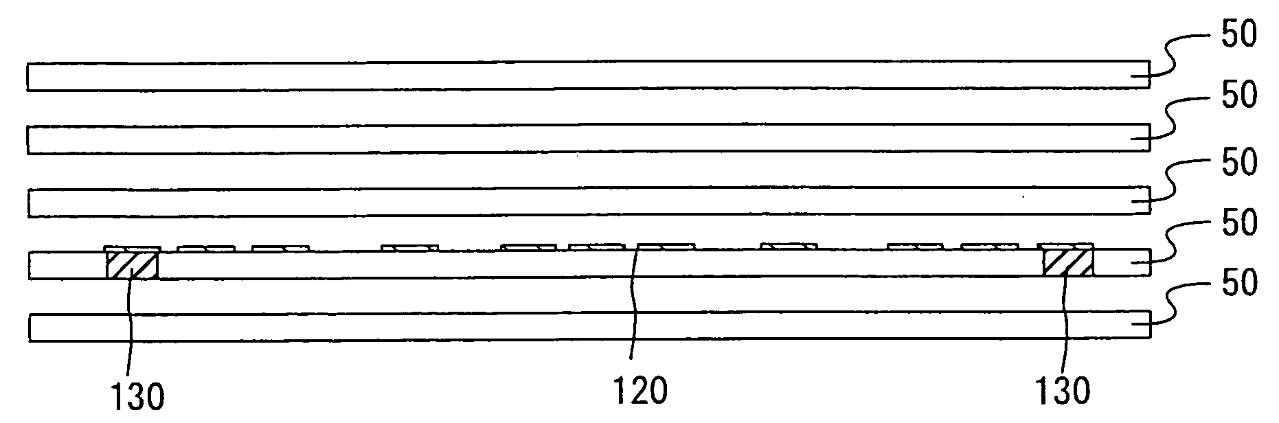
[0405] (1) The following paste was used to perform formation by a doctor blade method, so as to form a green sheet 50 having a thickness of 0.47 μm: a paste obtained by mixing 100 parts by weight of aluminum nitride powder (manufactured by Tokuyama Corp., average particle diameter: 0.6 μm), 4 parts by weight of alumina, 11.5 parts by weight of an acrylic resin binder, 0.5 part by weight of a dispersant and 53 parts by weight of alcohols of 1-butanol and ethanol.

[0406] (2) Next, this green sheet 50 was dried at 80° C. for 5 hours, and subsequently portions which would be conductor filled through holes 13a were formed by punching.

[0407] (3) The following were mixed to prepare a conductor containing paste A: 100 parts by weight of tungsten carbide particles having an average particle diameter of 1 μm, 3.0 parts by weight of an acrylic resin binder, 3.5 parts by weight of α-terpineol solvent, and 0.3 part by weight of a dispersant.

[...

example 2

Production of Ceramic Heater (See FIGS. 3, 4 and 6)

[0419] (1) A composition made of 100 parts by weight of aluminum nitride powder (average particle diameter: 0.6 μm), 4 parts by weight of yttria (average particle diameter: 0.4 μm), 12 parts by weight of an acrylic resin binder and an alcohol was subjected to spray-drying to form granular powder.

[0420] (2) Next, this granular powder was put into a mold and formed into a flat plate form to obtain a raw formed body (green).

[0421] (3) next, this raw formed body was hot-pressed at 1800° C. and a pressure of 20 MPa to yield a nitride aluminum plate having a thickness of 3 mm.

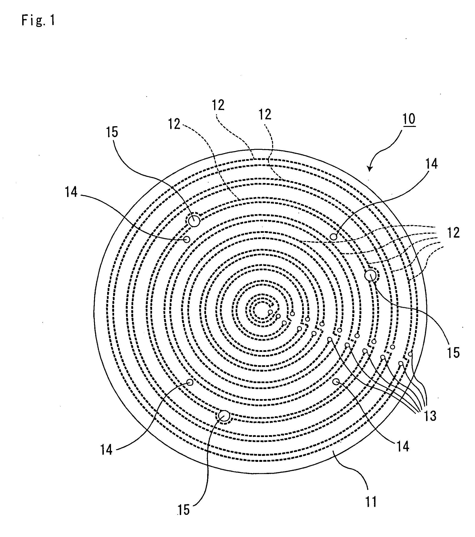
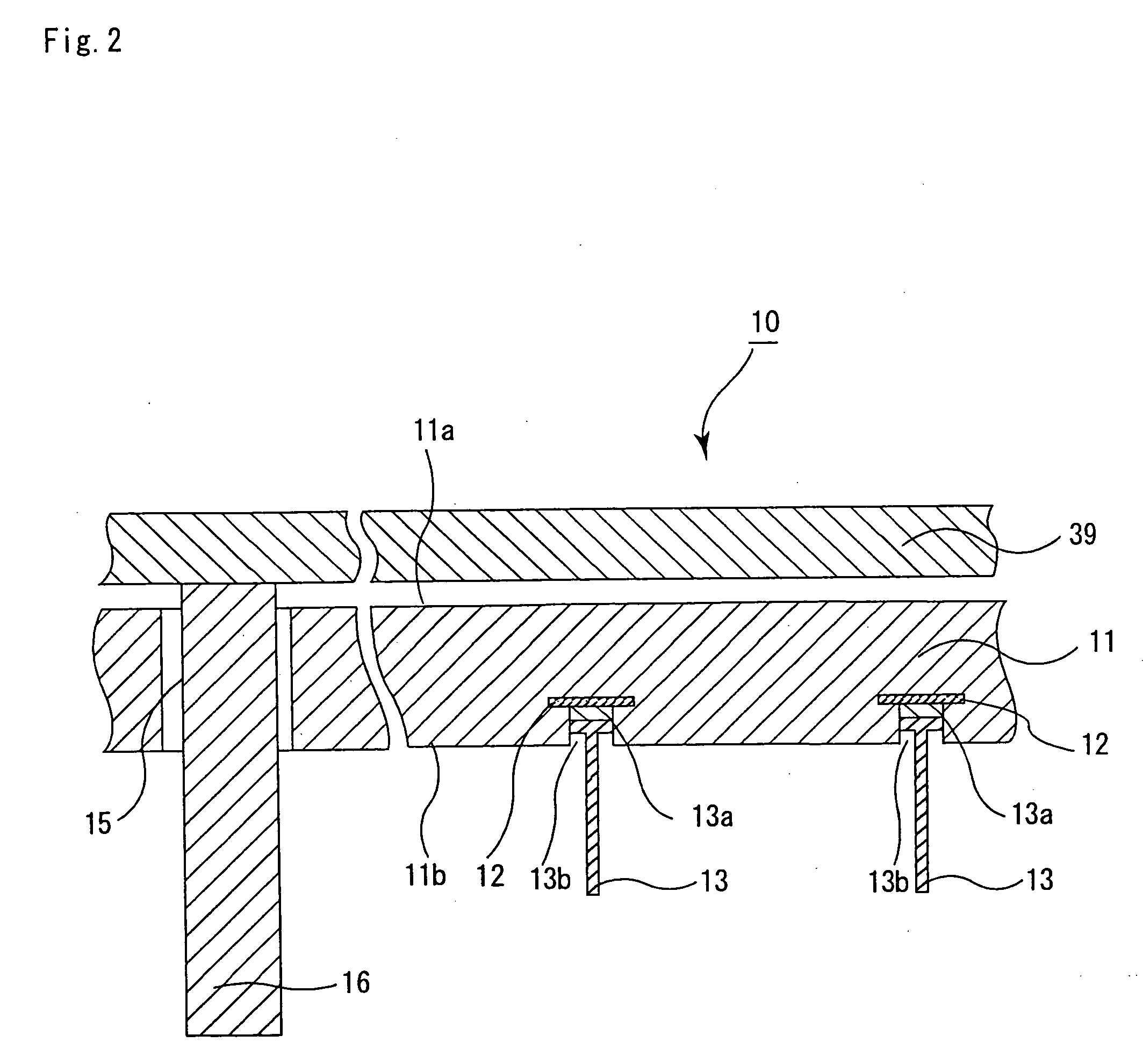
[0422] Next, this plate was cut out into a disk having a diameter of 210 mm, so as to prepare a plate made of the ceramic (ceramic substrate 21). This ceramic substrate 21 was drilled to form three through holes 25 (diameter: 3.5 mm), for passing lifter pins 26 (diameter: 3 mm) through, and bottomed holes 24 for embedding thermocouples (see FIG. 6(a)).

[0423] The...

example 3

[0433] (1) The following paste was used to perform formation by a doctor blade method, so as to form a green sheet 50 having a thickness of 0.47 μm: a paste obtained by mixing 100 parts by weight of SiC powder (manufactured by Yakushima Denko, average particle diameter: 1.1 μm), 4 parts by weight of B4C, 11.5 parts by weight of an acrylic resin binder, 0.5 part by weight of a dispersant and 53 parts by weight of alcohols of 1-butanol and ethanol. Furthermore, 80 parts by weight of borosilicate glass having an average particle size of 1.0 μm, 5 parts by weight of polyethylene glycol and 15 parts by weight of alcohol were mixed to yield a glass paste. This glass paste was applied to the formed green sheet.

[0434] (2) Next, this green sheet was dried at 80° C. for 5 hours, and subsequently portions which would be conductor filled through holes were formed by punching.

[0435] (3) The following were mixed to prepare a conductor containing paste A: 100 parts by weight of tungsten carbide ...


PUM

PropertyMeasurementUnit
Lengthaaaaaaaaaa
Diameteraaaaaaaaaa
Diameteraaaaaaaaaa

Abstract

A ceramic heater capable of stably supporting a semiconductor safer and evenly heating the whole of a semiconductor wafer or the like without generating any warp in the semiconductor wafer or the like. The ceramic heater includes a disk-like ceramic substrate, a heating element formed on a surface of or inside the ceramic substrate, and through holes for letting lifter pins pass through the ceramic substrate. The number of the formed through holes is three or more, and the through holes are formed in an area whose distance from the center of the ceramic substrate is ½ or more of the distance from the center to the outer edge of the ceramic substrate.

Description

TECHNICAL FIELD [0001] The present invention mainly relates to a ceramic heater and a ceramic bonded body which are used in the production and inspection of semiconductors, the field of optics, and so on. BACKGROUND ART [0002] Conventionally, a heater, wafer prober or the like wherein a base material made of a metal such as stainless steel or aluminum alloy is used has been used in semiconductor producing / inspecting devices and so on, examples of which include an etching device and a chemical vapor phase growth device and the like. [0003] However, such a heater made of metal has the following problems. [0004] First, the thickness of the heater plate must be as thick as about 15 mm since the heater is made of a metal. Because in a thin metal plate, a bend, a strain and so on are generated on the basis of thermal expansion resulting from heating so that a silicon wafer put on the metal plate is damaged or inclined. However, if the thickness of the heater plate is made thick, a problem...

Claims


Application Information

Patent Timeline
IPC IPC(8): C04B35/56C04B35/58C23C16/46H01L21/00H01L21/683H05B3/14
CPCB32B18/00H05B3/143B32B2311/08C04B35/56C04B35/5626C04B35/565C04B35/581C04B35/6264C04B35/62655C04B35/63C04B35/6303C04B35/634C04B35/645C04B37/025C04B2235/3201C04B2235/3217C04B2235/3227C04B2235/3284C04B2235/3296C04B2235/3409C04B2235/3418C04B2235/365C04B2235/3821C04B2235/3826C04B2235/3865C04B2235/606C04B2235/94C04B2237/04C04B2237/40C04B2237/403C04B2237/408C04B2237/50C04B2237/62C04B2237/704C23C16/46H01L21/67103H01L21/6833B32B38/145H05B3/20
Inventor ITO, YASUTAKA
Owner IBIDEN CO LTD
Why Eureka
Try Eureka