Light emitting device

Active Publication Date: 2005-03-03
EPISTAR CORP
View PDF19 Cites 16 Cited by
  • Summary
  • Abstract
  • Description
  • Claims
  • Application Information

AI Technical Summary

Benefits of technology

[0012] Because the first superlattice structure can spread carriers, and the carriers can tunnel the second superlattice st

Problems solved by technology

The major technical concerns is to seek low and stable operating forward voltage (Vf), since it is not easy to form ohmic contact between the indium tin oxide and p type GaN.
However, the agent layer between the indium tin oxide and the p type GaN contact layer will absorb output light intensity, and the forward voltage is unstable during operation beca

Method used


Image

  • Light emitting device
  • Light emitting device

Examples


Example

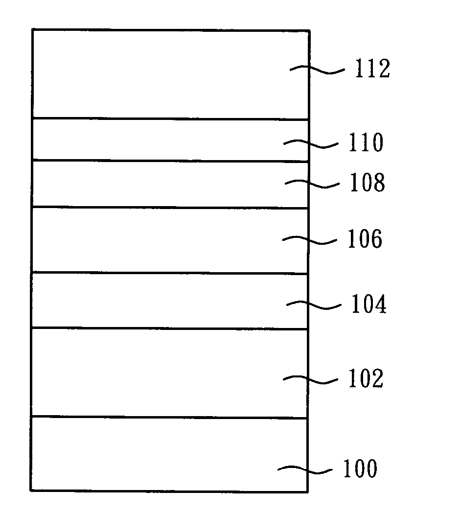
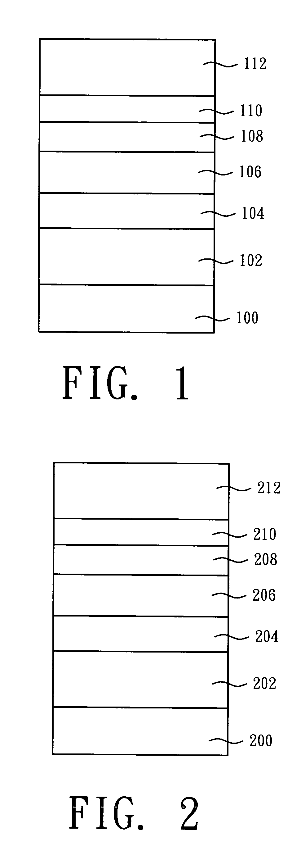
[0016] The present invention discloses a light emitting device comprising a contact layer composed of a hybrid superlattice structure which can spread hole carriers and provide tunneling contact for the carriers. In addition, an oxide transparent layer can be directly deposited on the contact layer. Therefore, the brightness of the light emitting device can be enhanced, and a stable and low forward voltage can be obtained. In order to make the illustration of the present invention more explicitly and completely, the following description is stated with reference to the accompanying drawings of FIG. 1 and FIG. 2.

[0017] Referring to FIG. 1, FIG. 1 illustrates a cross-sectional view of a light emitting device in accordance with a preferred embodiment of the present invention. The light emitting device structure of the present invention comprises a substrate 100 which is transparent, a n type semiconductor layer 102, an active layer 104, a p type cladding layer 106, a superlattice stru...


PUM


Abstract

A light emitting device is disclosed. The light emitting device comprises a contact layer and an oxide transparent layer located directly on the contact layer. The contact layer has a stacked structure formed by alternately stacking a plurality of nitride semiconductor layers having a wider bandgap and a plurality of nitride semiconductor layers having a narrower bandgap.

Description

FIELD OF THE INVENTION [0001] The present invention relates to a light emitting device, and more particularly, to a semiconductor light emitting device having high brightness and a low forward voltage. BACKGROUND OF THE INVENTION [0002] The metal oxide transparent conductive material, like indium tin oxide (ITO), nickel oxide (NiO) has been widely used on opto-electronic devices, such as thin film transistor liquid crystal display (TFT-LCD), organic light emitting device (OLED) and light emitting device especially in InGaN series material. It is used as a conductive window layer of the opto-electronic device for current spreading and light transmission. The major technical concerns is to seek low and stable operating forward voltage (Vf), since it is not easy to form ohmic contact between the indium tin oxide and p type GaN. [0003] The forward voltage is lowered by applying an agent layer between the indium tin oxide and p type GaN. For example, the U.S. Pat. No. 5,977,566 filed by ...

Claims


Application Information

Patent Timeline
IPC IPC(8): H01L29/22H01L29/24H01L33/04H01L33/14H01L33/32
CPCH01L33/04H01L33/14H01L33/32
Inventor TU, CHUAN-CHENGYOUNG, CHENG-CHUNGHUANG, PAO-IWU, JEN-CHAU
Owner EPISTAR CORP
Why Eureka
Try Eureka