Memory cell unit, nonvolatile semiconductor device, and liquid crystal display device including the nonvolatile semiconductor device

a memory cell and nonvolatile semiconductor technology, applied in semiconductor devices, radio frequency controlled devices, electrical devices, etc., can solve the problems of inability to achieve the effect of preventing erroneous writing to the unselected memory cell, highly reliable and stably operable, and reducing the area of the memory cell

Inactive Publication Date: 2005-03-10
FUJO MASUOKA +1
View PDF1 Cites 18 Cited by
  • Summary
  • Abstract
  • Description
  • Claims
  • Application Information

AI Technical Summary

Benefits of technology

[0023] According to the second inventive aspect, the memory cell unit is electrically connected to the semiconductor substrate, and the distance between the third impurity diffusion layer and the source diffusion layer is greater than the distance between the impurity diffusion layers disposed on the opposite sides of each of the memory cells. Therefore, the punch-through of the second selection transistor can be prevented when the writing prevention voltage is applied between the source diffusion layer and the third impurity diffusion layer. Therefore, when a writing operation is performed on a memory cell adjacent to the third impurity diffusion layer, the channel potential of the other unselected memory cell can be kept at the writing prevention voltage. Hence, erroneous writing to the unselected memory cell can assuredly be prevented, so that the memory cell unit is highly reliable and stably operable.
[0024] Where a distance between the drain diffusion layer and the second impurity diffusion layer is greater than the distance between the impurity diffusion layers disposed on opposite sides of each of the memory cells, punch-through of the first selection transistor can be prevented when the writing prevention voltage is applied between the drain diffusion layer and the second impurity diffusion layer. Therefore, when the writing operation is performed on a memory cell adjacent to the second impurity diffusion layer, the channel potential of the other unselected memory cell can be kept at the writing prevention voltage. Hence, erroneous writing to the unselected memory cell can assuredly be prevented, so that the memory cell unit is highly reliable and stably operable.
[0025] Where a plurality of memory cell units are arranged in a matrix configuration and each comprise either of the memory cell units described above, the selection transistors of the memory cell units each have a breakdown voltage not lower than the writing prevention voltage to be applied between the drain diffusion layer and the source diffusion layer. Particularly, when the writing operation is performed on the memory cell adjacent to the third impurity diffusion layer, the channel potential of the unselected memory cell can be kept at the writing prevention voltage. Hence, erroneous writing to the unselected memory cell can assuredly be prevented. Therefore, a nonvolatile semiconductor storage device can be provided which is highly reliable and stably operable.
[0026] As described above, the present invention is further directed to a nonvolatile semiconductor storage device, which includes a selection transistor having a sufficiently high breakdown voltage with respect to a bit line writing prevention voltage to be applied when electrons are injected into a charge storage layer of a memory cell, and is capable of assuredly preventing erroneous writing to an unselected memory cell.
[0027] Alternatively, a plurality of memory cell units are longitudinally and transversely arranged in a matrix configuration, and each comprise either of the memory cell units described above. A plurality of control gate lines are each provided by sequentially connecting control gates of memory cells provided in column-shaped semiconductor layers arranged longitudinally in each column of the matrix configuration, and are commonly connected. A plurality of bit lines are each provided by connecting drain diffusion layers of memory cell units provided in column-shaped semiconductor layers arranged transversely in each row of the matrix configuration. In this case, selection transistors of the memory cell units each have a breakdown voltage not lower than the writing prevention voltage to be applied between the drain diffusion layer and the source diffusion layer of the memory cell unit. Particularly, when the writing operation is performed on a memory cell adjacent to the third impurity diffusion layer, the channel potential of the unselected memory cell can be kept at not lower than the writing prevention voltage. Hence, erroneous writing to the unselected memory cell can assuredly be prevented. Therefore, a nonvolatile semiconductor device can be provided, which is highly reliable and stably operable.
[0028] Where an inventive liquid crystal display device comprises either of the semiconductor storage devices described above, erroneous writing to the semiconductor device can assuredly be prevented. Therefore, the liquid crystal display device is high reliable and stably operable.

Problems solved by technology

Therefore, how to reduce the area of the memory cells and how to increase the capacitance between the floating gate and the control gate are critical issues.
However, the thickness reduction of the gate insulation film has limitation in consideration of the reliability.
However, this approach poses a problem associated with the reliability and, hence, is not practical.
However, this is obstructive to the reduction of the area of the memory cells for the increase of the storage capacity of the EEPROM.
The back bias effect limits the number of memory cells to be connected in series on the device, thereby posing a problem associated with the increase of the storage capacity.
That is, the threshold voltages of the respective memory cells are liable to be non-uniform due to variation in an in-plane back bias effect of the semiconductor substrate.
The variations in the threshold voltages depending on the positions of the memory cells adversely influence write / erase / read voltages to be applied for the writing, erasing and reading operations with respect to the memory cells.
However, the aforesaid patent publications teach nothing about breakdown voltages of the selection transistors with respect to the bit line writing prevention voltage.
Hence, there is a possibility that a writing error occurs if the breakdown voltage VB1 is lower than the voltage VH4.
Hence, there is a possibility that a writing error occurs if the breakdown voltage VB1 is lower than the writing prevention voltage VH4.
Hence, there is a possibility that a writing error occurs if the breakdown voltage VB2 is lower than the writing prevention voltage VH4.

Method used


Image

  • Memory cell unit, nonvolatile semiconductor device, and liquid crystal display device including the nonvolatile semiconductor device
  • Memory cell unit, nonvolatile semiconductor device, and liquid crystal display device including the nonvolatile semiconductor device
  • Memory cell unit, nonvolatile semiconductor device, and liquid crystal display device including the nonvolatile semiconductor device

Examples


first embodiment

[0075] First Embodiment

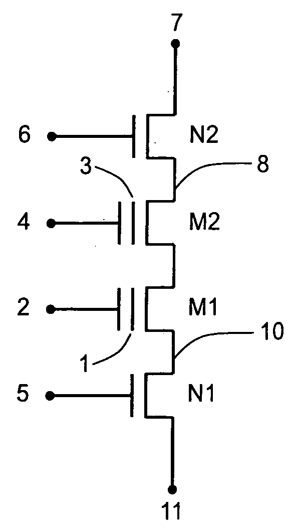
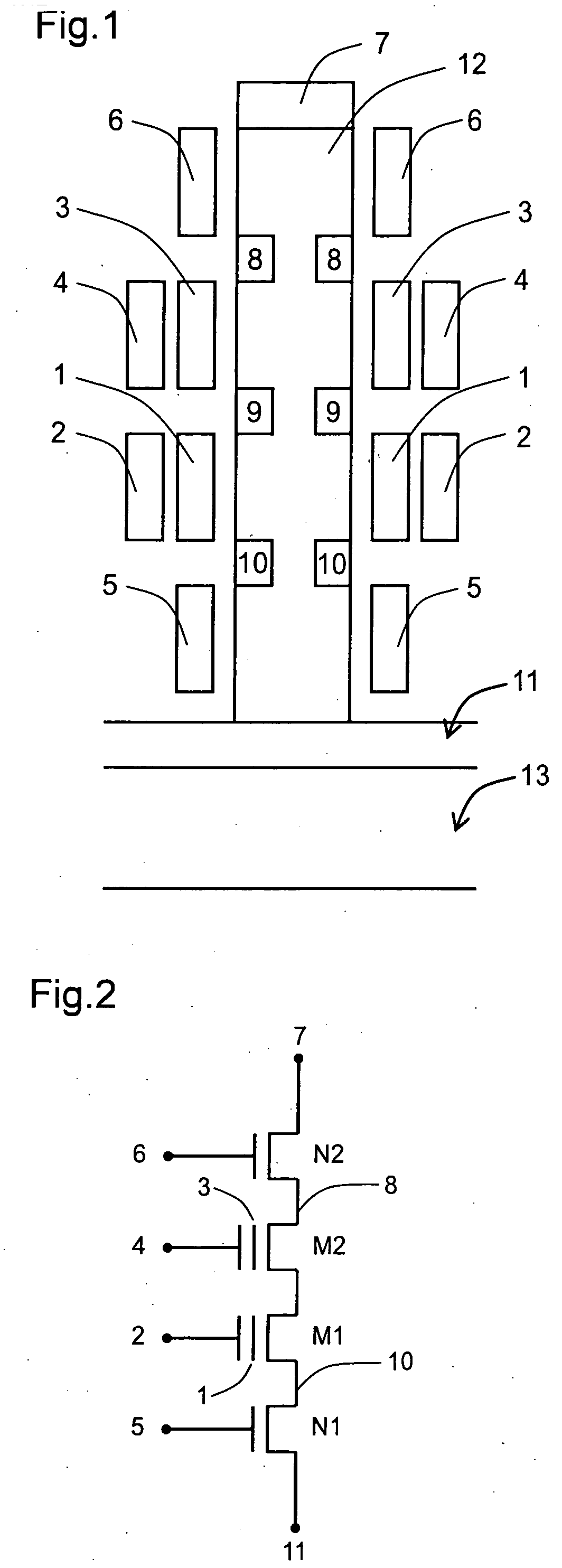
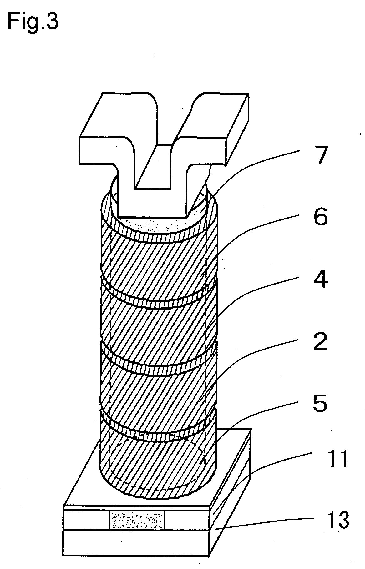
[0076] With reference to FIGS. 5 to 24, an explanation will be given to an exemplary production process for producing NAND memory cell units provided in a nonvolatile semiconductor storage device according to the present invention. The NAND memory cell units to be produced in this embodiment each include an island semiconductor layer formed, for example, by processing a semiconductor substrate into a sea-island configuration and having a peripheral surface serving as an active region, selection transistors provided in association with upper and lower portions of the island semiconductor layer, and a plurality of memory cells (e.g., two memory cells) arranged in series along the island semiconductor layer between the selection transistors and each including a floating gate constituted by a tunnel oxide film and a charge storage layer provided on the active region of the island semiconductor layer. The island semiconductor layer is electrically floated from the ...

second embodiment

[0096] Second Embodiment

[0097]FIG. 25 is a block diagram illustrating a memory cell unit array including NAND memory cell units of FIG. 1 arranged in a matrix configuration. FIG. 26 is an equivalent circuit diagram of the memory cell unit array. As shown in FIGS. 25 and 26, there are NAND memory cell units Paa, Pab to Pac, Pad selected by selection gate lines SG1a, SG2a and control gate lines CG1a, CG2a, NADN memory cell units Pba, Pbb to Pbc, Pbd selected by selection gate lines SG1b, SG2b and control gate lines CG1b, CG2b, NAND memory cell units Pca, Pcb to Pcc, Pcd selected by selection gate lines SG1c, SG2c and control gate lines CG1c, CG2c, and NAND memory cell units selected by selection gate lines SG1d, SG2d and control gate lines CG1d, CG2d. Further, there are provided bit lines BLa to BLd and a common source line SL crossing the selection gate lines and the control gate lines. An explanation will hereinafter be given to writing operations to be performed on a memory cell of...

third embodiment

[0110] Third Embodiment

[0111]FIG. 29 illustrates an exemplary memory cell unit array having substantially the same construction as the memory cell unit array shown in FIG. 25 but having a plurality of control gate lines shared by memory cells in different memory cell unit groups. FIG. 30 is an equivalent circuit diagram of the memory cell unit array. In the memory cell unit array shown in FIG. 25, one control gate selector transistor should be provided for each row of column-shaped semiconductor layers arranged along a control gate line in a space having a width as measured along a bit line for the row of column-shaped semiconductor layers. On the other hand, the memory cell unit array shown in FIG. 29 is advantageous in that an interconnection routing pitch of control gate lines is increased by connecting each two control gate lines to one common line and one control gate selector transistor is disposed in a space having a width as measured along a bit line for two rows of column-s...


PUM

PropertyMeasurementUnit
threshold voltageaaaaaaaaaa
thicknessaaaaaaaaaa
depthaaaaaaaaaa

Abstract

A memory cell unit including: a semiconductor substrate having a source diffusion layer provided in a surface thereof; a column-shaped semiconductor layer provided on the source diffusion layer and having a drain diffusion layer provided in an uppermost portion thereof; a memory cell arrangement which includes a plurality of memory cells arranged in series with the intervention of a first impurity diffusion layer; a first selection transistor connected to one end of the memory cell arrangement with the intervention of a second impurity diffusion layer and connected to the drain diffusion layer; and a second selection transistor connected to the other end of the memory cell arrangement with the intervention of a third impurity diffusion layer and connected to the source diffusion layer; wherein a distance between the third impurity diffusion layer and the source diffusion layer is greater than a distance between impurity diffusion layers disposed on opposite sides of each of the memory cells, whereby punch-through of the second selection transistor is prevented when a writing prevention voltage is applied between the source diffusion layer and the first impurity diffusion layer.

Description

CROSS-REFERENCE TO RELATED APPLICATION [0001] This application is related to Japanese application No.2003-315492 filed on Sep. 8, 2003 whose priority is claimed under 35 USC §119, the disclosure of which is incorporated by reference in its entirety. BACKGROUND OF THE INVENTION [0002] 1. Field of the Invention [0003] The present invention relates to a memory cell unit, a nonvolatile semiconductor storage device and a liquid crystal display device including the nonvolatile semiconductor storage device. [0004] 2. Description of the Related Art [0005] Exemplary memory cells of a known EEPROM are of a MOS transistor structure, which includes a gate portion including a charge storage layer and a control gate and is adapted to inject electric charges into the charge storage layer and release the electric charges from the charge storage layer by utilizing a tunnel current. The memory cells each store data “0” and “1” on the basis of a difference in threshold voltage attributable to a differ...

Claims


Application Information

Patent Timeline
Patent Type & Authority Applications(United States)
IPC IPC(8): G02F1/133H01L21/8247H01L27/115H01L29/768H01L29/786H01L29/788H01L29/792
CPCH01L27/11556H01L27/115H10B41/27H10B69/00H01L29/0611H10B41/41
Inventor MASUOKA, FUJIOSAKURABA, HIROSHIMATSUOKA, FUMIYOSHIUENO, SYOUNOSUKE
Owner FUJO MASUOKA
Why Eureka
Try Eureka