Undercoating material for wiring, embedded material, and wiring formation method

a technology of embedded materials and wiring, which is applied in the direction of photosensitive materials, photo-taking processes, instruments, etc., can solve the problems of deterioration of the pattern resolution of the resist, increased dielectric constant, and easy deterioration of the surface of the resist, so as to prevent deterioration of the resist pattern, reduce the damage to the substrate, and easy to remove

Active Publication Date: 2005-04-07
TOKYO OHKA KOGYO CO LTD
View PDF18 Cites 39 Cited by
  • Summary
  • Abstract
  • Description
  • Claims
  • Application Information

AI Technical Summary

Benefits of technology

(2) When recovery of the substrate is necessary due to deficient lithography, the undercoating layer can be easily removed by wet treatment with less damage to the substrate, and thus rework treatment for recovery of the substrate can be carried out reliably and easily. As a result, the problem of substrate regeneration treatment made difficult by a silicon-containing resist or an underc

Problems solved by technology

Such an entrance of the reflected light into the photoresist layer results in deterioration of the patterning resolution of the photoresist.
However, a material having such low dielectric constant is poor in resistance to O2 plasma ashing so that by exposure to O2 plasma, its surface is easily deteriorated, or the dielectric constant is increased.
When the conventional anti reflective coating film is formed on a semiconductor substrate having the dielectric layer of such low dielectric constant, O2 plasma ashing for removing the anti reflective coating layer may cause deterioration such as corrosion of the dielectric layer or rise in the electric constant, and as a result, there arises a problem that the electric characteristics of the wiring layer are adversely affected.
When these regulatory factors vary for some reason, there occurs patterning insufficiency, due to which the lithographic step has to be conducted again.
In this case, disposal of the semiconductor substrate and use of a new semiconductor substrate lead to waste of resources and exert an adverse effect on the environment.
Discussing the conventional anti reflective coating film from the viewpoint of such rework treatment, the conventional anti reflective coating layer is not suitable because there is a problem that it should be removed by O2 plasma ashing easily causing deterioration in the characteristics of a semiconductor substrate after rework treatment.
On the other hand, such a thin resist layer results in difficulty in maintaining the resistance of the resist layer in the step of etching the undercoating layer using the resist pattern as the mask, and disadvantageous effect in the etching resolution of the wiring layer or the wiring groove.
However, a material having such low dielectric constant is poor in resistance to O2 plasma ashing so that by exposure to O2 plasma, its surface is easily deteriorated, or the dielectric constant is increased.
When a resist pattern made of the conventional silicon bilayer resist is formed on a semiconductor substrate having the dielectric layer of such low dielectric constant to form a wiring layer, O2 plasma ashing for removing the undercoating layer on the substrate may cause deterioration such as corrosion of the dielectric layer or rise in the electric constant, and as a result, there arises a problem that the electric characteristics of the wiring layer are adversely affected.
When these regulatory factors vary for some reason, there occurs patterning insufficiency, due to which the lithographic step has to be conducted again.
In this case, disposal of the semiconductor substrate and use of a new semiconductor substrate lead to waste of resources and exert an adverse effect on the environment.
Discussing the conventional undercoating layer from the viewpoint of such rework treatment, the conventional undercoating layer is not suitable because there is a problem that it should be removed by O2 plasma ashing easily causing deterioration in the characteristics of a semiconductor substrate after rework treatment.
Accordingly, even if the conventional anti reflective coating film is employed as the undercoating layer in the silicon bilayer resist, the problem attributable to removal of the undercoating layer cannot be solved.
However, a material having such low dielectric constant is poor in resistance to O2 plasma ashing so that by exposure to O2 plasma, its surface is easily deteriorated, or the dielectric constant is increased.
When a resist pattern made of the conventional multilayer resist is formed on a semiconductor substrate hav

Method used


Image

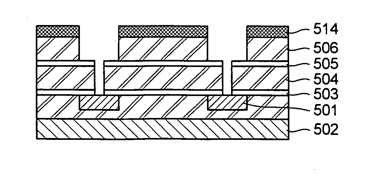
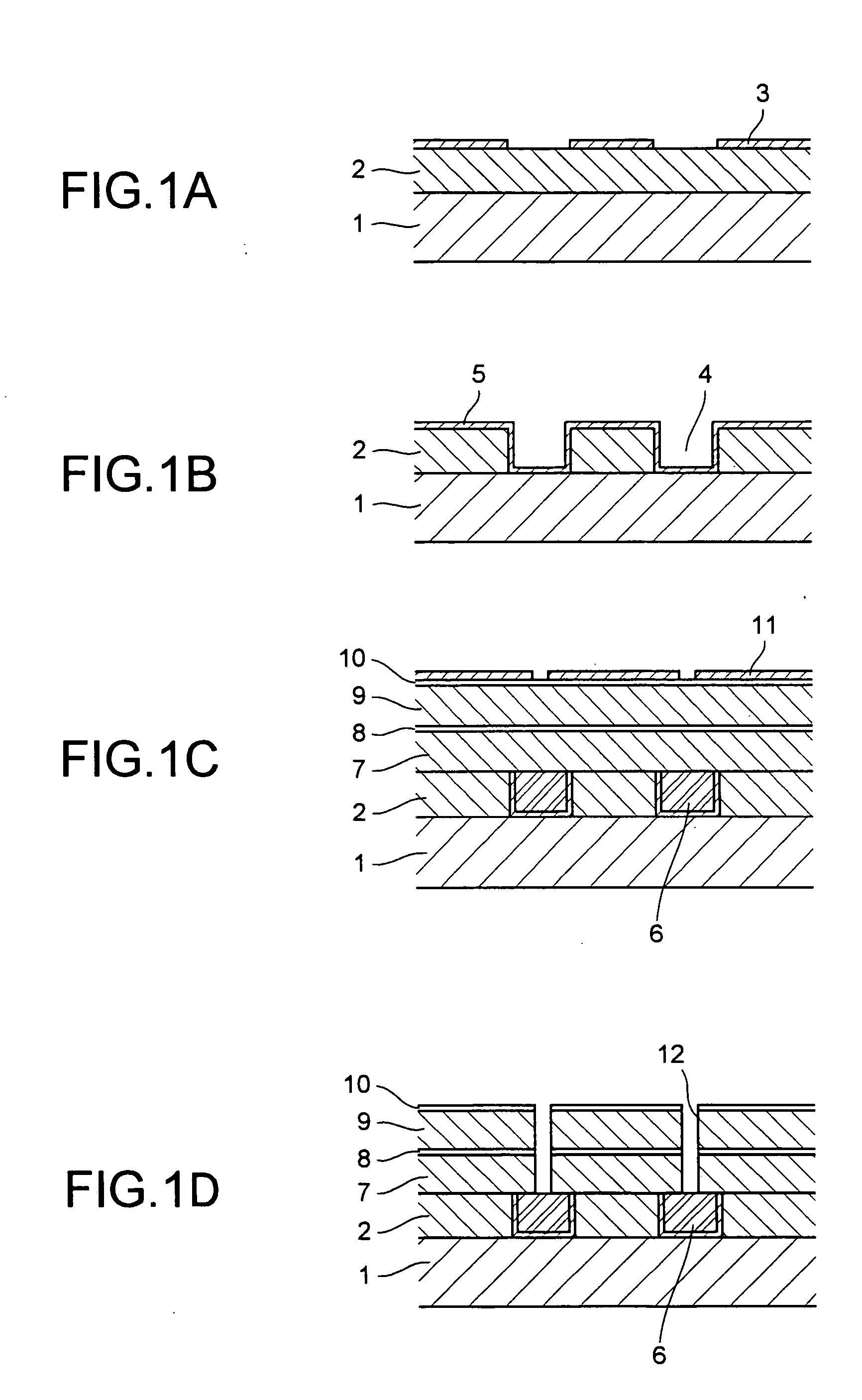
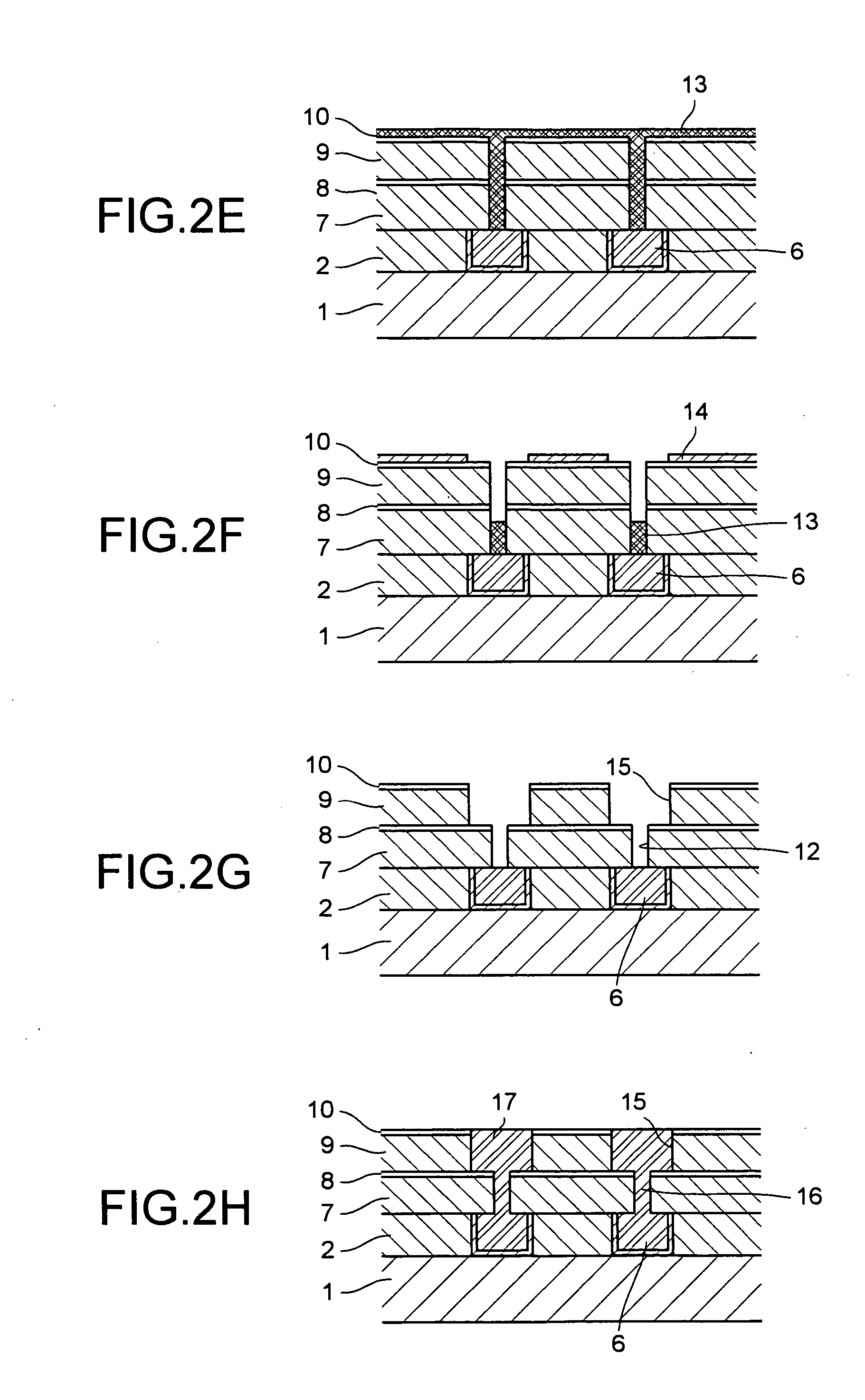
  • Undercoating material for wiring, embedded material, and wiring formation method
  • Undercoating material for wiring, embedded material, and wiring formation method
  • Undercoating material for wiring, embedded material, and wiring formation method

Examples


examples 1 to 4

The following resin compositions (A), (B), (C), and (D) were prepared as the undercoating materials.

(A) A resin composition with a solid content adjusted to 6 wt %, produced by dissolving a resin component consisting of ethyl p-styrenesulfonate in a solvent consisting of γ-butyrolactone / ethyl lactate (2:8).

(B) A resin composition with a solid content adjusted to 6 wt %, produced by dissolving a resin component consisting of ethyl p-styrenesulfonate:hydroxyethyl acrylate (5:5), and Cymel 1172 (tetramethylol glycoluril by Mitsui Cyanamid Corporation) in an amount of 20 wt % based on the resin component, in a solvent consisting of ethyl lactate.

(C) A resin composition with a solid content adjusted to 6 wt %, produced by dissolving a resin component consisting of ethyl p-styrenesulfonate / 9-hydroxyanthracenyl acrylate (5:5), in a solvent consisting of γ-butyrolactone / ethyl lactate (2:8).

(D) A resin composition with a solid content adjusted to 6 wt %, produced by dissolving a res...

example 5

The resin composition (C) was additionally blended with an optical acid-generating agent TPS-109 (Midori Kagaku Corporation) in an amount of 3 wt % based on the resin component to prepare a new resin composition (C2). A wiring structure was formed in the same manner as in Example 1 except that the resin composition (C2) was used. As a result, a wiring structure having a rectangular pattern excellent in dimensional regulation was obtained.

examples 6 to 9

The following resin compositions (A), (B), (C), and (D) were prepared as the undercoating materials.

(A) A resin composition with a solid content adjusted to 6 wt %, produced by dissolving a resin component consisting of ethyl p-styrenesulfonate in a solvent consisting of γ-butyrolactone / ethyl lactate (2:8).

(B) A resin composition with a solid content adjusted to 6 wt %, produced by dissolving a resin component consisting of ethyl p-styrenesulfonate:hydroxyethyl acrylate (5:5), and Cymel 1172 (tetramethylol glycoluril by Mitsui Cyanamid Corporation) in an amount of 20 wt % based on the resin component, in a solvent consisting of ethyl lactate.

(C) A resin composition with a solid content adjusted to 6 wt %, produced by dissolving a resin component consisting of ethyl p-styrenesulfonate:9-hydroxyanthracenyl acrylate (5:5), in a solvent consisting of γ-butyrolactone / ethyl lactate (2:8).

(D) A resin composition with a solid content adjusted to 6 wt %, produced by dissolving a res...


PUM

PropertyMeasurementUnit
Temperatureaaaaaaaaaa
Timeaaaaaaaaaa
Dielectric polarization enthalpyaaaaaaaaaa

Abstract

This invention provides an undercoating layer material and a filler material containing a resin component having at least a substituent group which is capable of releasing a terminal group to form a sulfonic acid residue upon application of predetermined energy, and a solvent. The resin component has at least a repeating unit represented by formula (1):
wherein n is an integer of 1 or more, X represents a C1 to C10 linear or branched alkyl chain, an aromatic or alicyclic alkyl chain or an alkyl ester chain, and Y is a substituent group forming a sulfonic acid residue upon application of predetermined energy.

Description

BACKGROUND OF THE INVENTION 1) Field of the Invention The present invention relates to an undercoating material used preferably for forming wiring on a semiconductor substrate, a filler material and a wiring formation method using the same. The undercoating material referred to herein indicates (a) an undercoating layer which is formed on a substrate before formation of a photoresist layer on the substrate whereby a reflected exposure light from the surface of the substrate at the time of patterning of a photoresist is prevented from entering the photoresist, to achieve improvement in the resolution of the photoresist pattern, (b) an undercoating layer suitable for a silicon bilayer resist, which is characterized by improving the patterning accuracy of a resist by constituting a photoresist layer used in lithography for wiring, from two layers, that is, an undercoating layer including an organic film and a silicon-containing upper resist layer, and (c) an undercoating layer suitab...

Claims


Application Information

Patent Timeline
IPC IPC(8): G03F7/11G03F7/00G03F7/075G03F7/09H01L21/312H01L21/768
CPCG03F7/075G03F7/091H01L21/312Y10S430/145H01L21/76808Y10S430/146H01L21/76802H01L21/02118G03F7/11
Inventor NAKAMURA, ETSUKOWAKIYA, KAZUMASA
Owner TOKYO OHKA KOGYO CO LTD
Why Eureka
Try Eureka