Heterojunction bipolar transistor using reverse emitter window

a bipolar transistor and reverse emitter technology, applied in the field of semiconductor/solid-state device manufacturing, electrical equipment, basic electric elements, etc., can solve the problems of device performance problems, variations in performance, and the etching process inherently produces a rough surface on the substrate, so as to reduce the base resistance and increase the speed and noise performance of the hbt

Active Publication Date: 2005-04-14
CHARTERED SEMICONDUCTOR MANUFACTURING
View PDF11 Cites 42 Cited by
  • Summary
  • Abstract
  • Description
  • Claims
  • Application Information

AI Technical Summary

Benefits of technology

[0025] The HBT of the present invention overcomes the problems associated with over-etching, the detrimental effects of ion implantation and annealing, and inconsistency of manufacturability experienced in existing methods of manufacture of H...

Problems solved by technology

The etching process inherently produces a rough surface on the substrate since the etchants used are not particularly selective between the polysilicon layer forming the base structure and the underlying silicon substrate.
The rough surface causes a major problem because the growth of the compound semiconductive material is irregular and its thickness is not constant as a result of the roughness of the substrate.
This leads to performance problems with the device and variations in performance from device to device.
It also causes junction leakage and more power consumption.
The overlap is necessary to provide room for an emitter contact, but it causes another major problem with unwanted capacitance between the emitter and base structures.
However, variations in the size of the emitter contact lead to a further major problem causing performance variations in the HBT from device to device.
Several of these processes inherently damage the compound semiconductive material.
Etching polysilicon over a compound semiconductive layer, for example, adversely affects the compound semiconductive material because the etchants used do not selectively etch only the polysilicon.
Some of the compound semiconductive material is also etched during this processing, resulting in HBTs that exhibit relatively poor noise performance and in leakage current, which in turn reduces integrated circuit yield.
The adverse effects of etching the ...

Method used


Image

  • Heterojunction bipolar transistor using reverse emitter window
  • Heterojunction bipolar transistor using reverse emitter window
  • Heterojunction bipolar transistor using reverse emitter window

Examples


Embodiment Construction

[0054] In the following description, numerous specific details are given to provide a thorough understanding of the invention. However, it will be apparent to one skilled in the art that the invention may be practiced without these specific details. In order to avoid obscuring the present invention, some well-known system configurations, and processes are not disclosed in detail.

[0055] Likewise, the drawings showing embodiments of the apparatus are semi-diagrammatic and not to scale and, particularly, some of the dimensions are for the clarity of presentation and are shown greatly exaggerated in the FIGs. Generally, the device can be operated in any orientation.

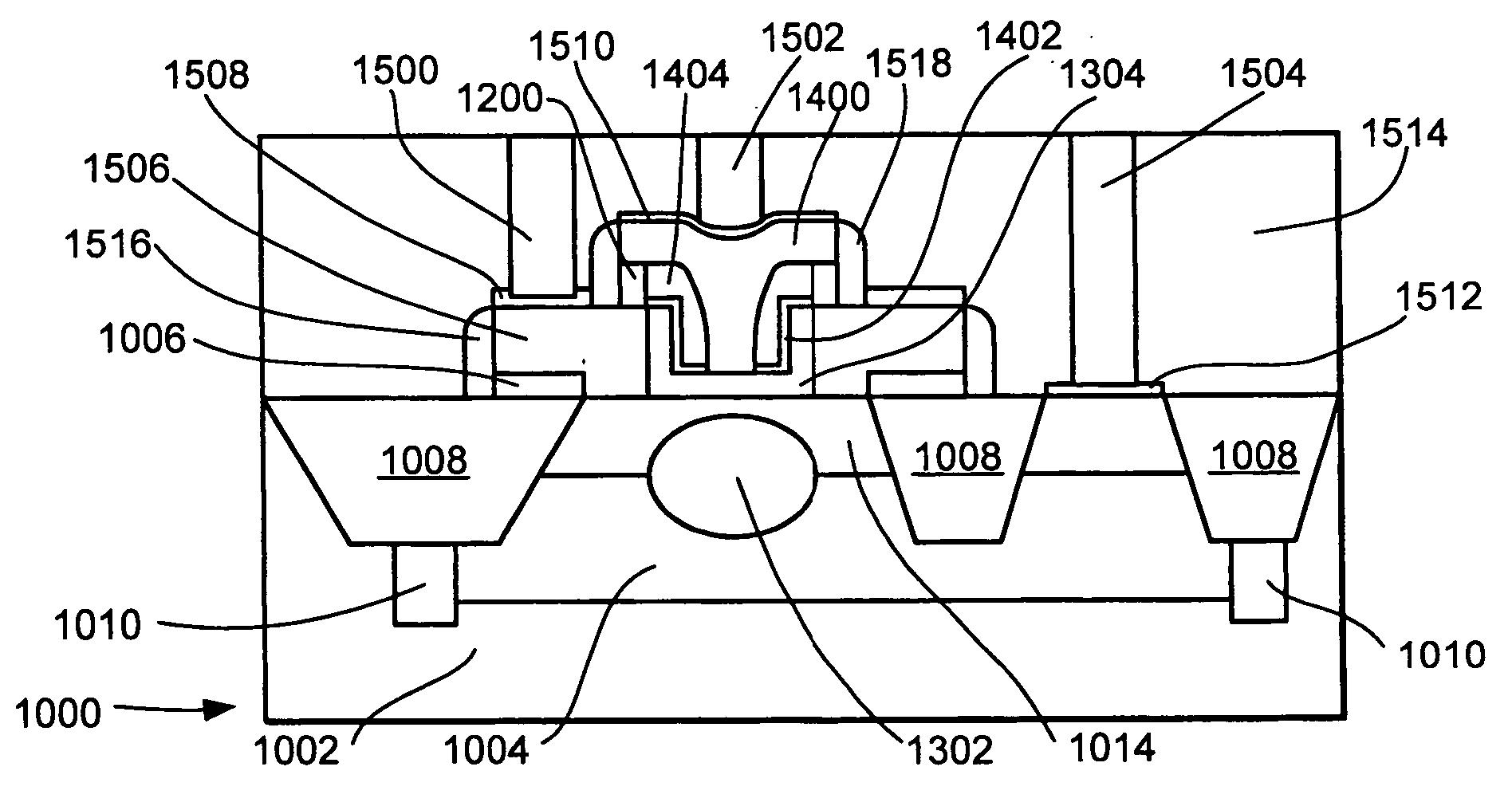
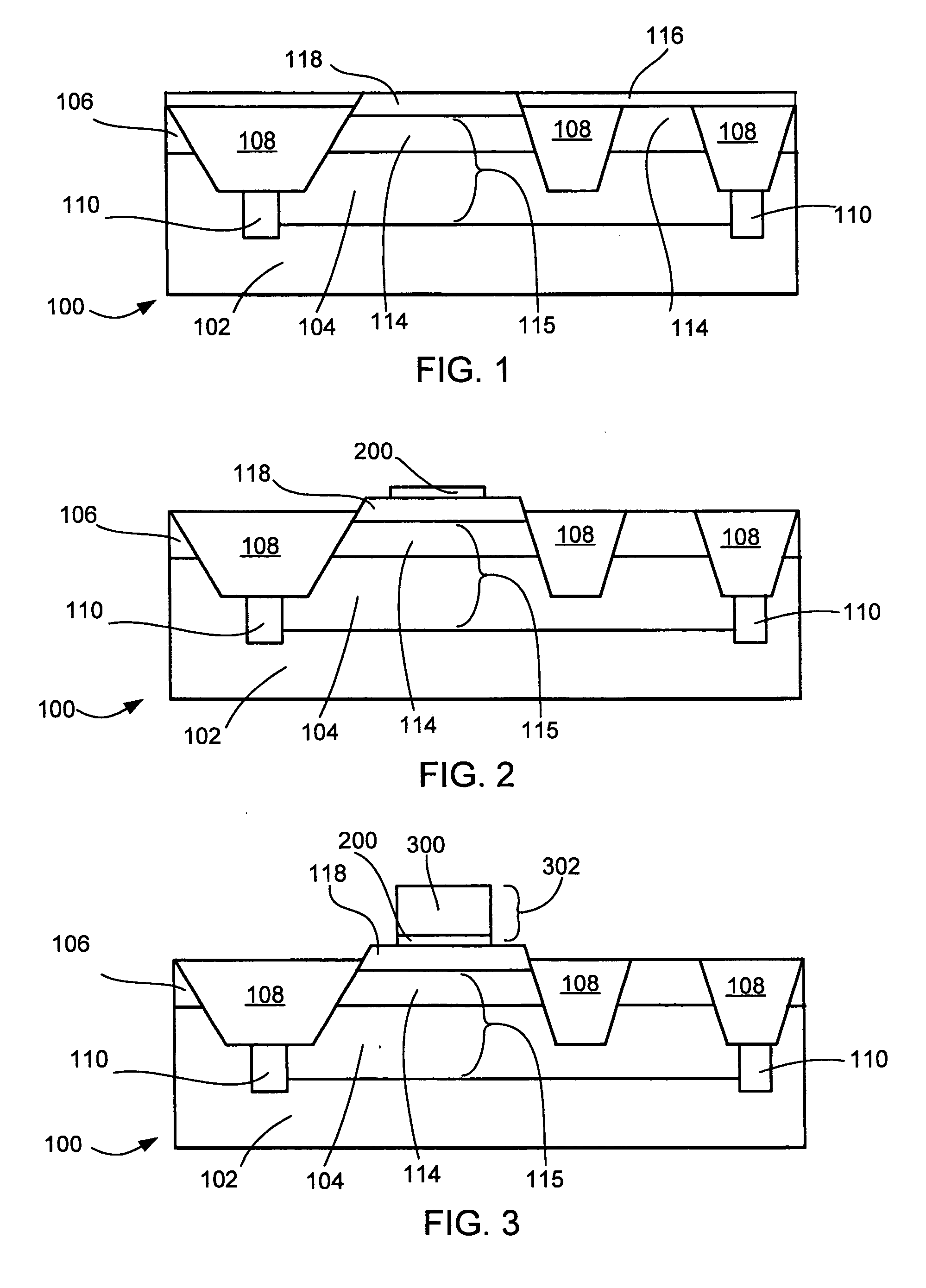
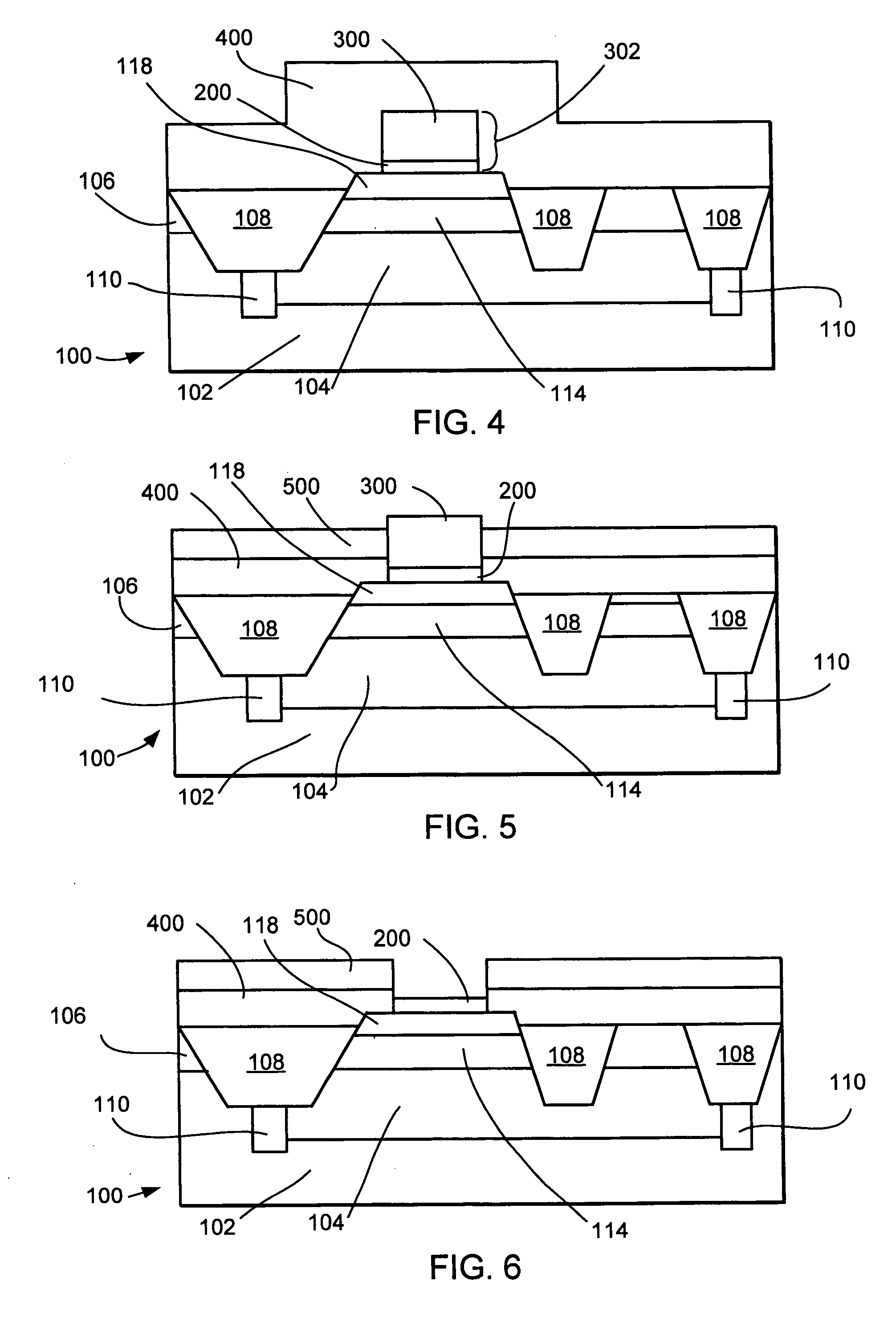
[0056] Referring now to FIG. 1, therein is shown a cross-sectional view of a heterojunction bipolar transistor (HBT) 100 in an intermediate stage of manufacture in accordance with the present invention using a selective deposition method. A semiconductor substrate 102 has been implanted with a dopant to form a buried collec...


PUM


Abstract

A heterojunction bipolar transistor (HBT), and manufacturing method therefor, comprising a semiconductor substrate having a collector region, an intrinsic base region of a compound semiconductive material over the collector region, an extrinsic base region, an emitter structure, an interlevel dielectric layer over the collector region, extrinsic base region and emitter structure, and connections through the interlevel dielectric layer to the base region, the emitter structure, and the collector region. The emitter structure is formed by forming a reverse emitter window over the intrinsic base region, which subsequently is etched to form an emitter window having a multi-layer reverse insulating spacer therein.

Description

TECHNICAL FIELD [0001] The present invention relates generally to semiconductor technology and more specifically to a method and apparatus for manufacturing heterojunction bipolar transistors. BACKGROUND ART [0002] A bipolar junction transistor (BJT) is a three-terminal device that can controllably vary the magnitude of the electrical current that flows between two of the terminals. The three terminals include a base terminal, a collector terminal, and an emitter terminal. The movement of electrical charge carriers, which produce electrical current flow between the collector and the emitter terminals, varies dependent upon variations in the voltage on the base terminal thereby causing the magnitude of the current to vary. Thus, the current flow through the emitter and collector terminals is controlled by the voltage across the base and emitter terminals. The terminals of a BJT are connected to their respective base, collector, and emitter structures formed in a semiconductor substra...

Claims


Application Information

Patent Timeline
IPC IPC(8): H01L21/331H01L29/08H01L29/417H01L29/737
CPCH01L29/0821H01L29/7378H01L29/66242H01L29/41708
Inventor VERMA, PURAKH RAJCHU, SHAO-FU SANFORDCHAN, LAPLI, JIAN XUNZHENG, JIA ZHEN
Owner CHARTERED SEMICONDUCTOR MANUFACTURING
Why Eureka
Try Eureka