High frequency power amplifier circuit and electronic component for high frequency power amplifier

a high frequency power amplifier and electronic component technology, applied in low noise amplifiers, amplification control device circuits, gain control, etc., can solve the problems of increasing power consumption, increasing costs, and affecting the performance of high-frequency power amplifiers, so as to improve the high-frequency power amplifying characteristic, reduce the scattering of characteristic between modules, and improve the effect of high-frequency power amplifying characteristics

Active Publication Date: 2005-04-21
MURATA MFG CO LTD
View PDF6 Cites 49 Cited by
  • Summary
  • Abstract
  • Description
  • Claims
  • Application Information

AI Technical Summary

Benefits of technology

[0014] (9) Furthermore, a high frequency amplifier circuit that uses a bipolar transistor instead of the FETs Q0 and Q1 in the circuit of FIG. 12 is also supposed. By using the bipolar transistor, a fault due to a short channel effect can be prevented. In the bipolar transistor, however, instead of not obtaining the short channel effect in the FET, there is an Early effect that, even if a base-emitter voltage is kept constantly, as a collector-emitter voltage increases, an effective base width decreases and a collector current increases.
[0041] (22) Furthermore, according to the present invention, the controllability of a high frequency power amplifying characteristic is improved and the general-purpose use of a high frequency power amplifier circuit and a module that mounts the high frequency power amplifier circuit can be improved.

Problems solved by technology

Accordingly, a drain current (idle current) of the amplifying FET shifts from a desired value, and a desired high frequency power amplifying characteristic is not obtained, such as necessary output power is not output, and power consumption increases.
However, in that case, because the steps of accurately measuring an FET characteristic and adjusting the resistive element are required, a cost increase is incurred.
Besides, in a short channel FET, the channel modulation coefficient λ cannot be ignored even in a saturation area, and a power voltage slightly differs depending on a user system.
Accordingly, even if the shift of the bias point is corrected by adjusting the external resistive element, it became evident that an idle current of a desired size cannot apply to an amplifying FET due to the influence of λ when the power voltage differs depending on the user system to be used.

Method used


Image

  • High frequency power amplifier circuit and electronic component for high frequency power amplifier
  • High frequency power amplifier circuit and electronic component for high frequency power amplifier
  • High frequency power amplifier circuit and electronic component for high frequency power amplifier

Examples


embodiment 1

[Embodiment 1]

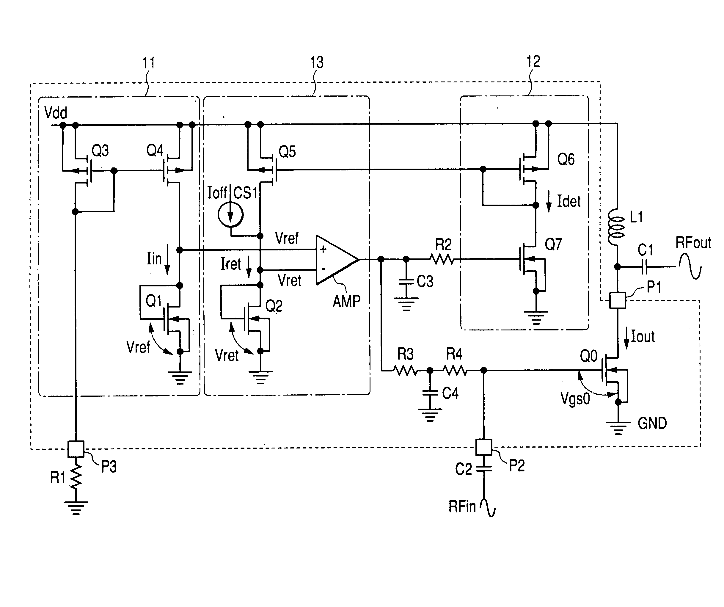
[0074] (25) FIG. 1 shows rough composition of a first embodiment of a high frequency power amplifier circuit according to the present invention. Although not limited in particular, for example, the three high frequency power amplifier circuits having such composition as the embodiment of FIG. 1 are connected in a cascade, and mounted on an insulating substrate, such as a ceramic substrate, together with an external resistive element or a capacitive element, thereby constructing an RF power module (refer to FIG. 9 and FIG. 10). Further, cascade connection means that the three power amplifier circuits are connected so that the previous-stage high frequency output is input to the next-stage input pin. The high frequency power amplifier circuit of each stage is the same as FIG. 1 as the composition respectively, but differs in the size (gate width) of an amplifying FET. An FET of a broader size is used in the order of the first stage, second stage, and third stage. In the ...

embodiment 2

[Embodiment 2]

[0103] (53) Next, a second embodiment of a high frequency power amplifier circuit according to the present invention is described with reference to FIG. 3.

[0104] A cellular phone of a GSM (global system for mobile communication) method is constructed so that the output power of the high frequency power amplifier circuit can be controlled by the output control voltage Vapc. FIG. 3 is an embodiment of the high frequency power amplifier circuit in which the output power control by such a Vapc is enabled. FIG. 3 differs from the high frequency power amplifier of the embodiment of FIG. 1 in that a bias current applied to the amplifying FET Q0 is kept constantly by specifying the current I in applied from the constant current circuits (Q3 and Q4) that construct the reference circuit 11 to the amplifying FET Q1 to be a predetermined current value (fixed). To the contrary, in this embodiment (FIG. 3), the idle current Iout applied to the amplifying FET Q0 varies by allowing t...

embodiment 3

[Embodiment 3]

[0109] (58) Next, a third embodiment of a high frequency power amplifier circuit according to the present invention is described with reference to FIG. 5.

[0110] This embodiment allows the high power amplifier circuit of the example of FIG. 3 to have two semiconductor chips and to provide a detection circuit (current sense circuit) for detecting output power (Power). The output power detection circuit in this embodiment has a detecting FET Q9 in which the same voltage as the voltage input to the gate pin of the amplifying FET Q0 is input to the gate pin through a resistor R5, a current mirror circuit 15 that transfers the drain current applied to the FET Q9, and an external resistor R6 that converts the current transferred from the current mirror circuit 15 into a voltage.

[0111] (59) The FET Q9 for detecting output power is an element of the same characteristic having the same gate length formed in the same process as the amplifying FET Q0 and is formed so as to have ...


PUM


Abstract

In a high frequency power amplifier circuit that supplies a bias to an amplifying FET by a current mirror method, scattering of a threshold voltage Vth due to the scattering of the channel impurity concentration of the FET, and a shift of a bias point caused by the scattering of the threshold voltage Vth and a channel length modulation coefficient λ due to a short channel effect are corrected automatically. The scattering of a high frequency power amplifying characteristic can be reduced as a result.

Description

CROSS-REFERENCE TO RELATED APPLICATION [0001] The present application claims priority from Japanese patent application No. 2003-356219 filed on Oct. 16, 2003, and No. 2003-356218 filed on Oct. 16, 2003, the contents of which are hereby incorporated by reference into this application. BACKGROUND OF THE INVENTION [0002] (1) The present invention relates to an effective technology for applying to a high frequency power amplifier circuit and an electronic component for a high frequency power amplifier that incorporates this high frequency power amplifier circuit, and, in particular, relates to a technology that realizes a stable amplifying characteristic in the high frequency power amplifier circuit for supplying an amplifying transistor with a bias by a current mirror method. [0003] (2) A high frequency power amplifier circuit (having multi-stage composition usually) that uses a semiconductor amplifying device, such as a MOSFET (insulated gate field-effect transistor) or a GaAs-MESFET ...

Claims


Application Information

Patent Timeline
Patent Type & Authority Applications(United States)
IPC IPC(8): H03F1/30H03G1/00
CPCH03F1/301H03F2200/294H03F2200/372H03G2201/40H03G2201/103H03G2201/206H03G2201/307H03G1/0005
Inventor TSURUMAKI, HIROKAZUNAGAI, HIROYUKIFURUYA, TOMIOISHIKAWA, MAKOTO
Owner MURATA MFG CO LTD
Why Eureka
Try Eureka