

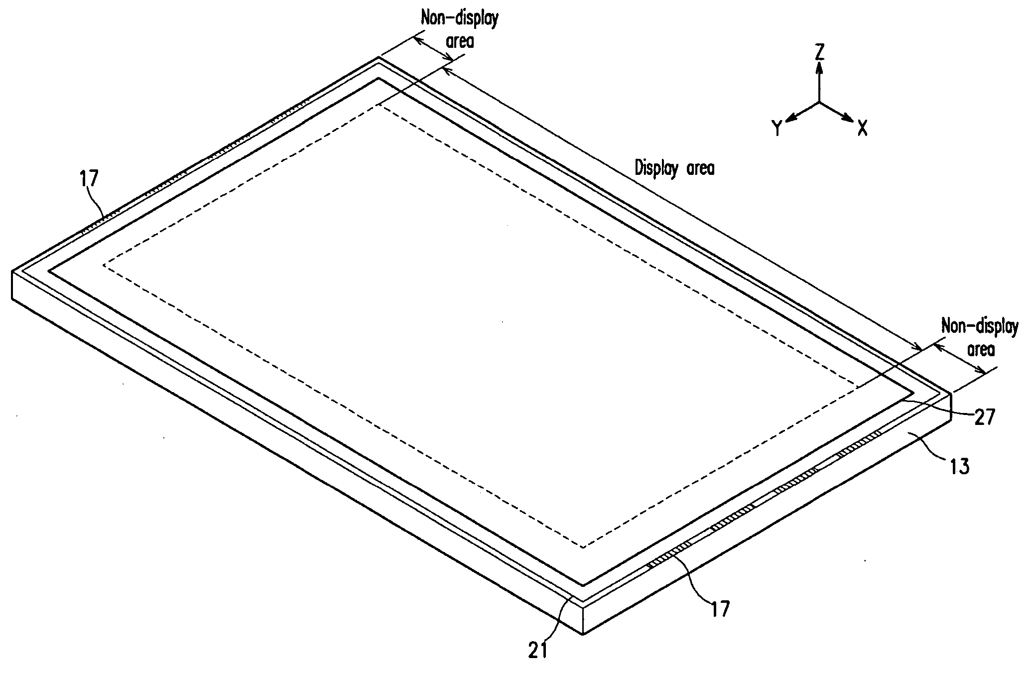
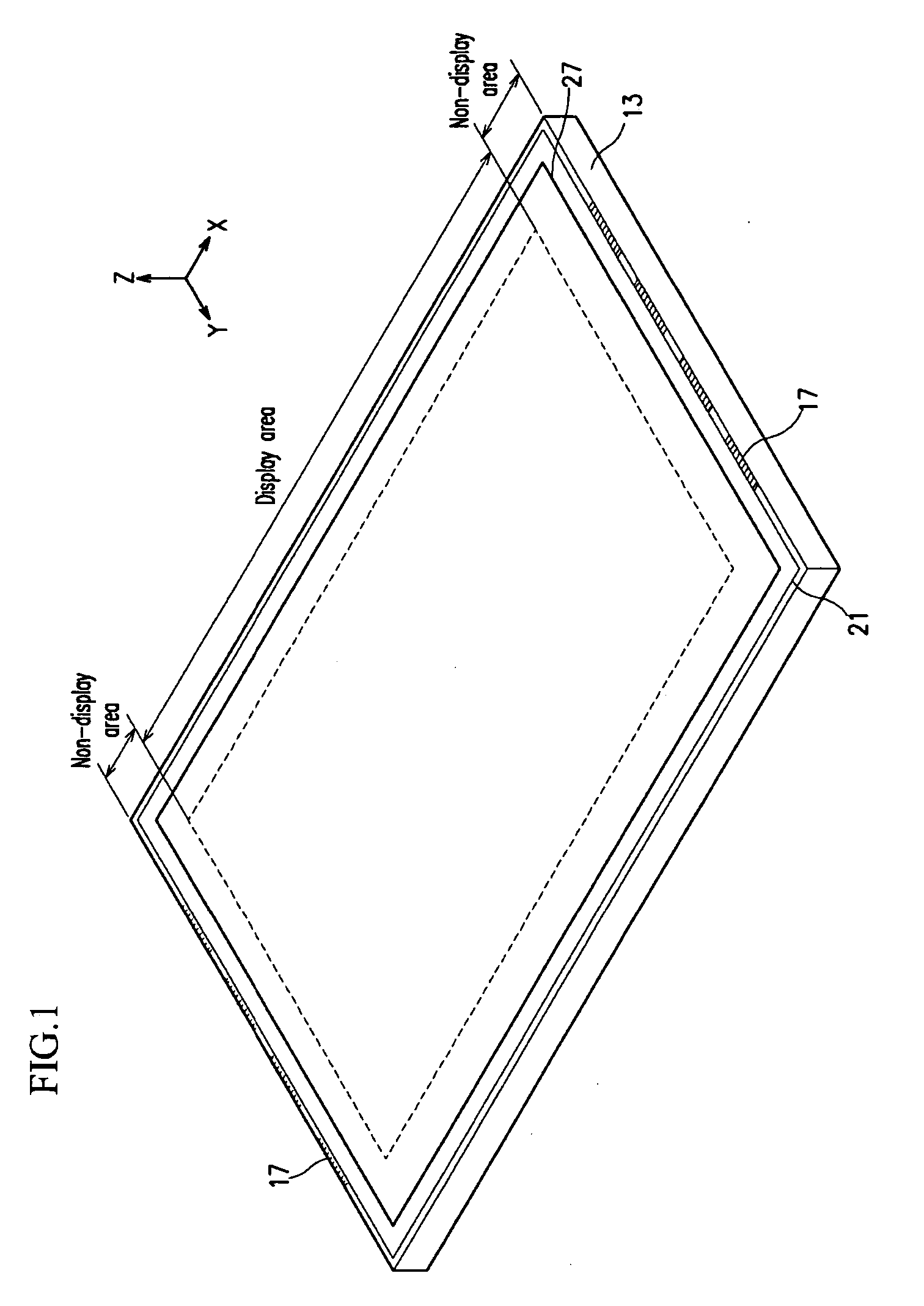
Plasma display panel provided with an improved protective layer
a technology of protective layer and display panel, which is applied in the manufacture of electric discharge tube/lamp, electrodes, and electrode systems, etc., can solve the problems of difficult control of a specific quantity of dopant, high unit cost of protection layer, etc., and achieve the effect of improving the operating characteristics of the same and improving the material properties and operating characteristics
- Summary
- Abstract
- Description
- Claims
- Application Information
AI Technical Summary
Benefits of technology
Problems solved by technology
Method used
Image

Examples
exemplary embodiment 1
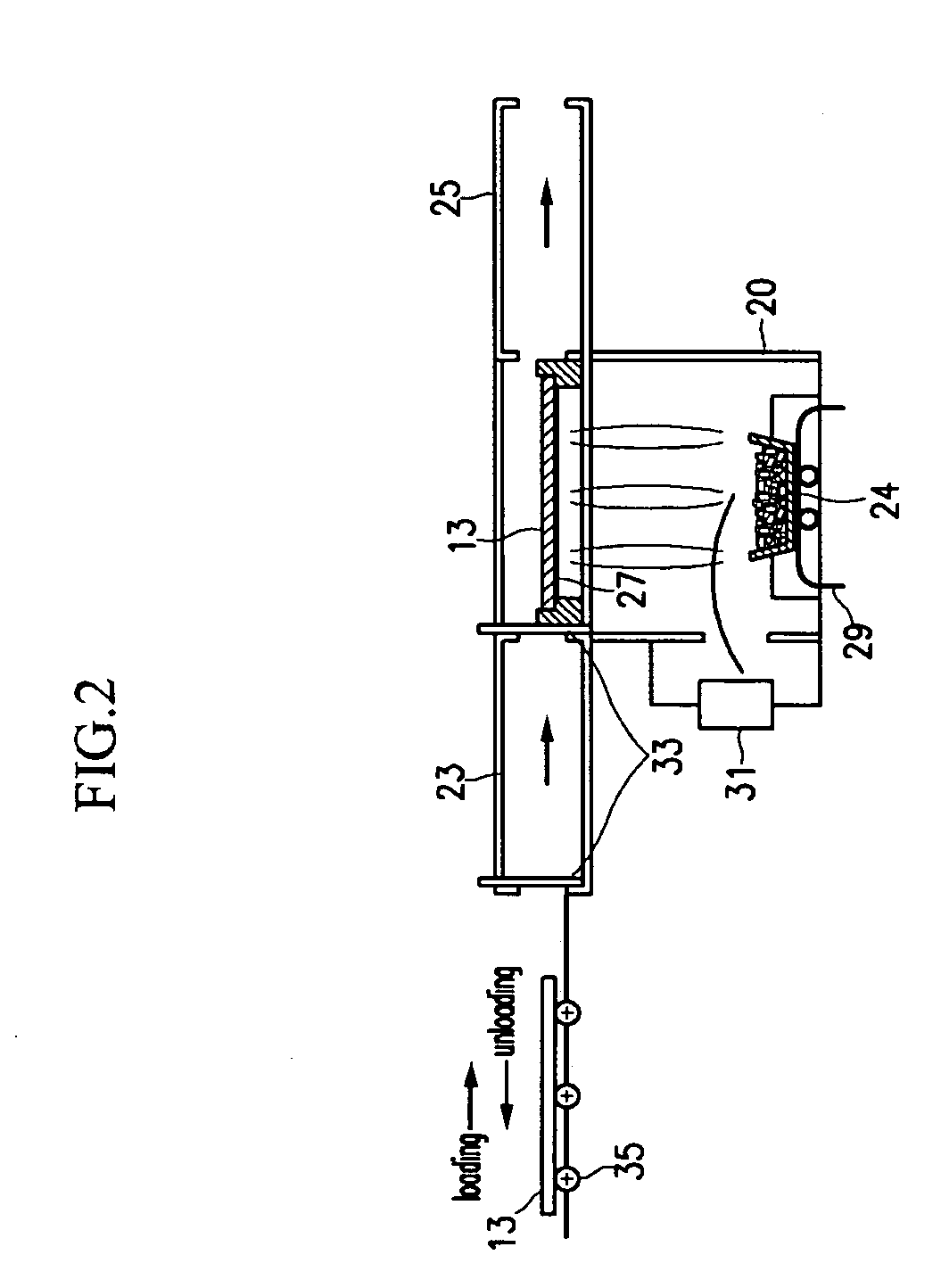
[0045] MgO pellets were placed in an MgO deposition chamber, and MgO was deposited on a PDP on which a dielectric layer had been formed. The resulting MgO protection layer was formed to a thickness of approximately 7000 Å. A standard pressure inside the deposition chamber was set at 1×10⁻⁴ Pa, and a pressure during deposition was set at 5.3×10⁻² Pa. Also, the substrate was maintained at 200±5° C. while supplying oxygen at a rate of 100 sccm. Electron beams were irradiated from an electron gun set at a current of 390 mA and a voltage of −15 kV to deposit the MgO protection layer. A partial pressure ratio of hydrogen and oxygen was set at approximately 6:1, and the grain size of the MgO protection layer was made to be approximately 250 nm to approximately 350 nm. Accordingly, the statistical delay times were measured while varying a mixing ratio of the (111) planes to the (110) planes. The results are shown in Table 2 below.
TABLE 2Mixing ratio of (111) planes to (110)planesStatistic...
exemplary embodiment 2
[0048] In this embodiment, the partial pressure ratio of hydrogen and oxygen was adjusted to approximately 3:1 to produce an MgO protection layer with a grain size of 200 nm to 250 nm. Therefore, the mixing ratio of the (111) planes to the (110) planes was settled, and the statistical delay times were measured. The results are shown in Table 3 below.
TABLE 3Mixing ratio of (111) planes to (110)planesStatistical delay time (ns)11:9403˜41422:8335˜34633:7253˜29244:6282˜33155:5323˜334
[0049] The information illustrated by Table 3 is exemplary and should not be understood as limiting the invention. Other embodiments may use other mixing ratios and / or provide other statistical delay times. As shown in Table 3, when the grain size of the MgO protection layer was approximately 200 nm to approximately 250 nm and the ratio of the (111) planes to the (110) planes of the MgO protection layer was determined through visual observation to be about 3:7, the statistical delay time was the shortest. ...
exemplary embodiment 3
[0051] The partial pressure ratio of hydrogen and oxygen was adjusted to approximately 2.5:1 to produce an MgO protection layer with a grain size of approximately 150 nm to 200 nm. Therefore, the mixing ratio of the (111) planes to the (110) planes was settled, and the statistical delay times were measured. The results are shown in Table 4 below. The remaining conditions were identical to those of Experimental Example 1.
TABLE 4Mixing ratio of (111) planes to (110)planesStatistical delay time (ns)11.5:8.5381˜41222.5:7.5323˜33233.5:6.5271˜28344.5:5.5352˜35755.5:4.5361˜383
[0052] The information illustrated by Table 4 is exemplary and should not be understood as limiting the invention. Other embodiments may use other mixing ratios and / or provide other statistical delay times. As shown in Table 4, when the grain size of the MgO protection layer is approximately 150 nm to 200 nm and the ratio of the (111) planes to the (110) planes of the MgO protection layer is determined through visua...
PUM
 Abstract
Description
Claims
Application Information