System for continuous growing of monocrystalline silicon

a monocrystalline silicon and continuous growth technology, applied in the direction of crystal growth process polycrystalline material growth, etc., can solve the problem that the adjacent wall is no longer driven to an excess temperature, and achieve improved thermal distribution, improved temperature control, and optimized thermal distribution

Active Publication Date: 2005-05-05
CORNER STAR LTD
View PDF39 Cites 49 Cited by
  • Summary
  • Abstract
  • Description
  • Claims
  • Application Information

AI Technical Summary

Benefits of technology

[0027] Another aspect of the invention provides enhanced temperature control that maintains a temperature in the melt of approximately 1420° C., such that the temperature has an optimized thermal distribution between the melt and crystal for accelerated crystal growth. To achieve such an optimized thermal distribution at the critical interface between the crystal and the melt, a plurality of annular, independently monitored heating elements are disposed in a radial pattern across the base of the growth crucible, as close to walls and to the bottom of the growth crucible as possible. The heating elements are separately controlled with active feedback to enable rapid thermal response and distribute the thermal workload to achieve an optimized thermal distribution across the interface between the crystal and the melt and between the crystal and walls of the crucible. This also contributes to improved crucible life, as well as reduction of oxygen and other impurities, in the finished single crystal silicon.
[0028] In contrast to a conventional

Problems solved by technology

Further, the region adjacent to the walls i

Method used


Image

  • System for continuous growing of monocrystalline silicon
  • System for continuous growing of monocrystalline silicon
  • System for continuous growing of monocrystalline silicon

Examples


Embodiment Construction

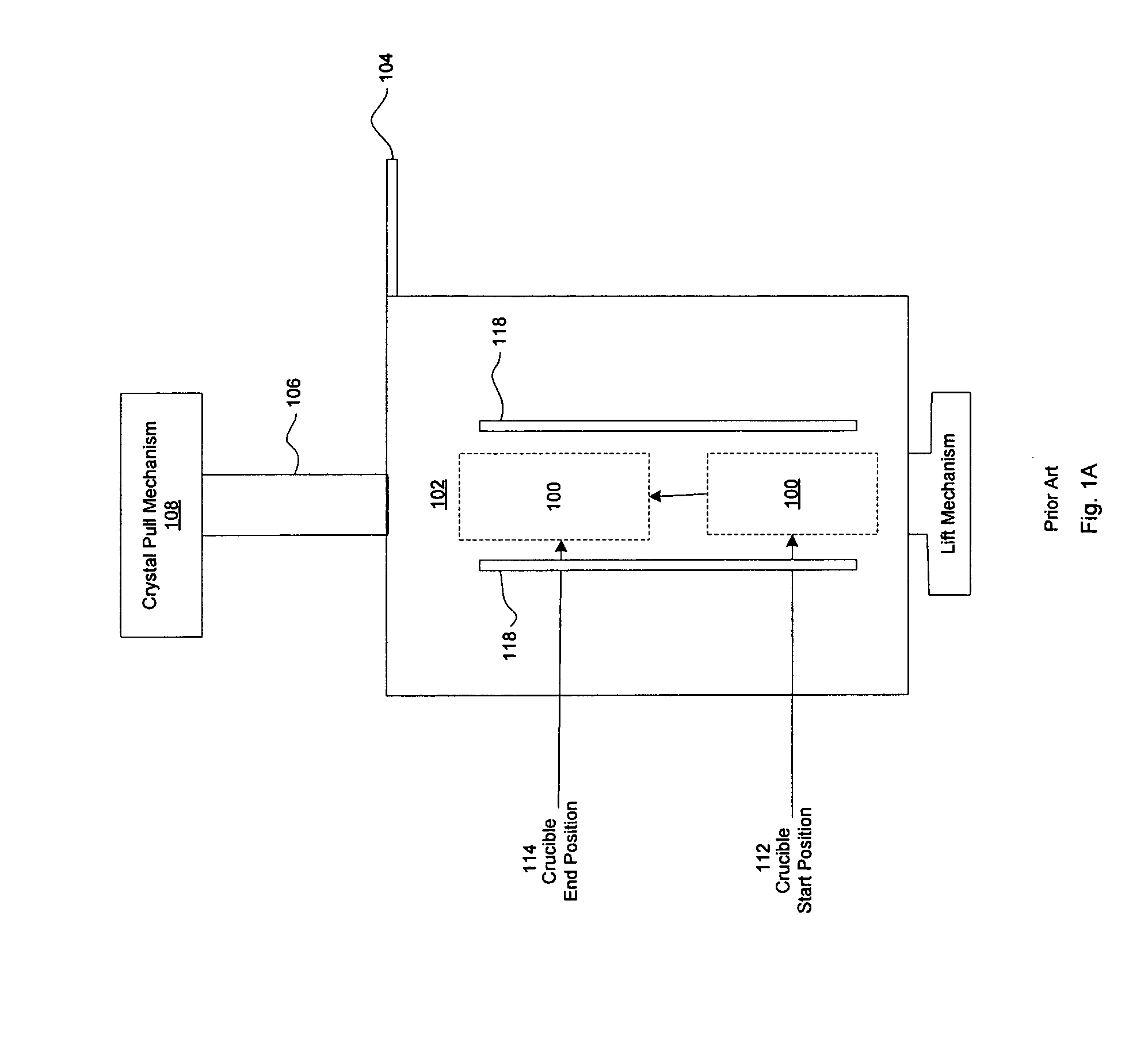
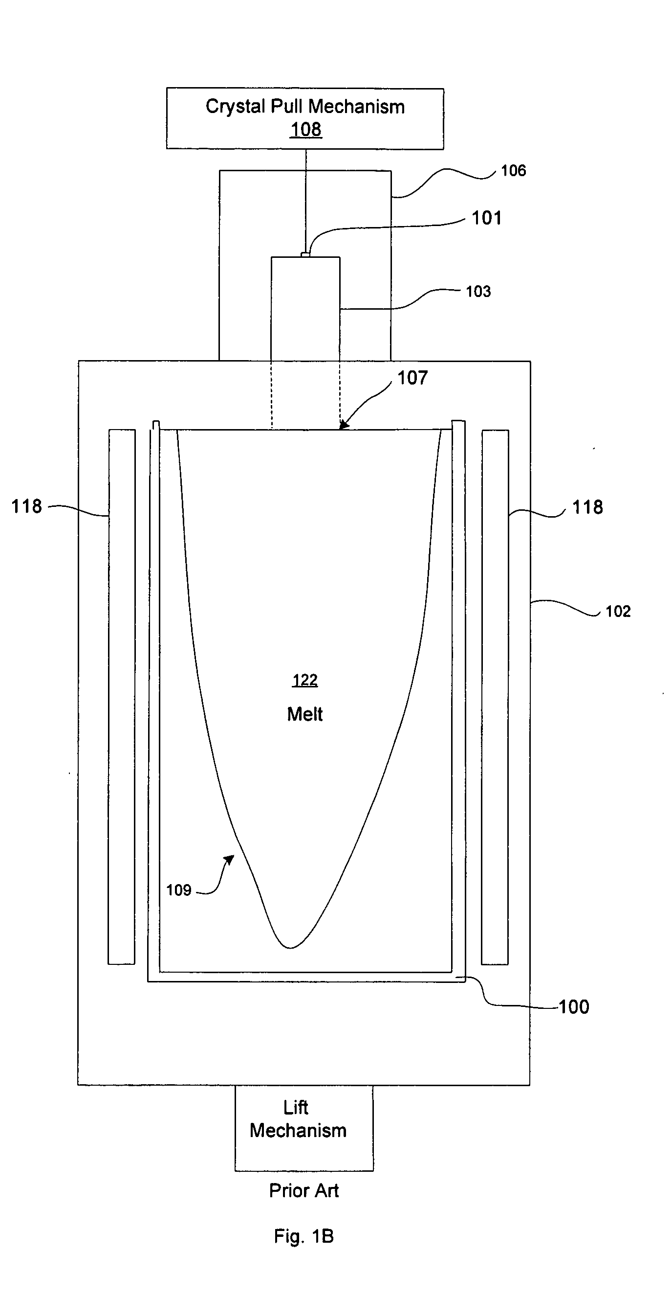
[0040] Referring to FIGS. 1A and 1B, in a conventional CZ system pieces of polysilicon are melted in a fused silica crucible 100 in an inert atmosphere in growth chamber 102. The atmosphere in the chamber 102 is typically argon and is controlled by isolation valve 104 in accordance with techniques that are well known. The silicon is held in crucible 100 at a temperature just above 1412 degrees C, the melting point of silicon. A high quality seed crystal with the desired crystalline orientation is lowered in the crystal pull chamber 106 to contact the melt at crystal melt interface 107 in the crucible 100 while being rotated. Crucible 100 is simultaneously rotated in the opposite direction to induce mixing in the melt and to attempt to minimize temperature non-uniformities. A portion of the seed crystal is dissolved in the molten silicon to remove strained outer portions and to expose fresh crystal surfaces.

[0041] The seed is then slowly raised or pulled from the melt in crystal pul...


PUM


Abstract

An improved system based on the Czochralski process for continuous growth of a single crystal ingot comprises a low aspect ratio, large diameter, and substantially flat crucible, including an optional weir surrounding the crystal. The low aspect ratio crucible substantially eliminates convection currents and reduces oxygen content in a finished single crystal silicon ingot. A separate level controlled silicon pre-melting chamber provides a continuous source of molten silicon to the growth crucible advantageously eliminating the need for vertical travel and a crucible raising system during the crystal pulling process. A plurality of heaters beneath the crucible establish corresponding thermal zones across the melt. Thermal output of the heaters is individually controlled for providing an optimal thermal distribution across the melt and at the crystal/melt interface for improved crystal growth. Multiple crystal pulling chambers are provided for continuous processing and high throughput.

Description

CROSS-REFERENCE TO RELATED APPLICATION [0001] This patent application claims the benefit of U.S. provisional patent application Ser. No. 60 / 517,124, filed Nov. 3, 2003, which is incorporated herein by reference.BACKGROUND [0002] 1. Field of the Invention [0003] The field of the invention generally relates to growing silicon crystals by the Czochralski (CZ) technique. In particular, the field of the invention relates to a system and method for continuous and rapid growing of ultra pure, high minority carrier lifetime mono-crystalline silicon based on improvements to the Czochralski method. [0004] 2. Background of Related Art [0005] Referring to FIGS. 1A and 1B, to be useful for the fabrication of semiconductor electronic components, silicon must be formed into a large (about 10-30 cm diameter), nearly perfect, single crystal, since grain boundaries and other crystalline defects degrade device performance. Sophisticated techniques are needed to obtain single crystals of such high qual...

Claims


Application Information

Patent Timeline
IPC IPC(8): C30B1/00C30B15/00C30B15/02C30B15/10C30B15/14C30B21/06C30B27/02C30B28/10C30B29/06C30B30/04
CPCC30B15/02Y10T117/1088C30B15/14C30B29/06Y10T117/1072Y10T117/108Y10T117/10Y10T117/1068Y10T117/1004Y10T117/1052Y10T117/1032Y10T117/1008Y10T117/1024Y10T117/1056Y10T117/1092C30B15/10H01L21/20C30B15/002C30B15/04C30B15/12C30B15/22
Inventor BENDER, DAVID L.
Owner CORNER STAR LTD
Why Eureka
Try Eureka