Semiconductor device and method for fabricating the same
a technology of semiconductors and capacitors, applied in the direction of transistors, solid-state devices, capacitors, etc., can solve the problems of body current increasing to a problematic extent in practice, and achieve the effect of reducing parasitic capacitance and improving operating speed
- Summary
- Abstract
- Description
- Claims
- Application Information
AI Technical Summary
Benefits of technology
Problems solved by technology
Method used
Image
Examples
embodiment 1
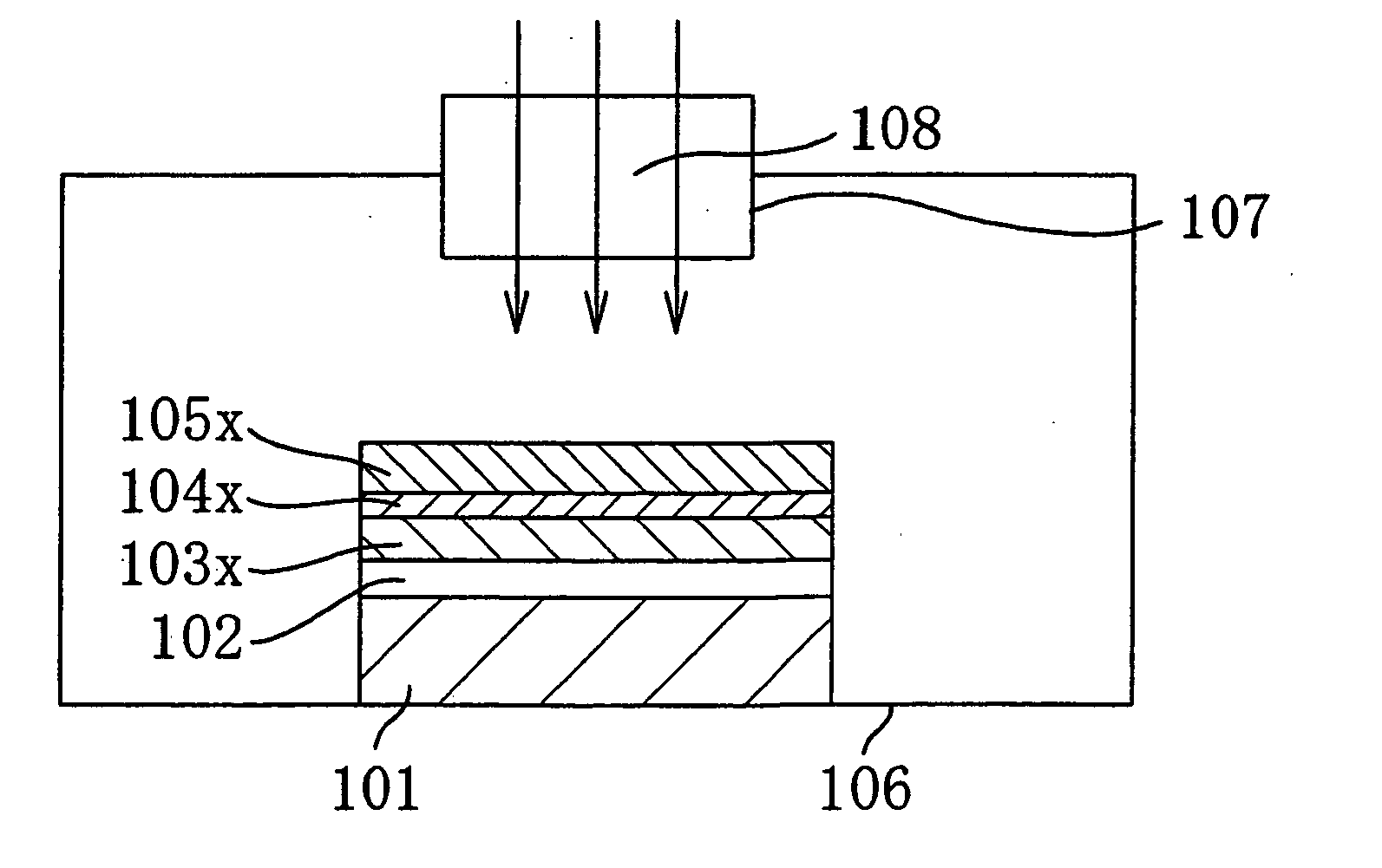
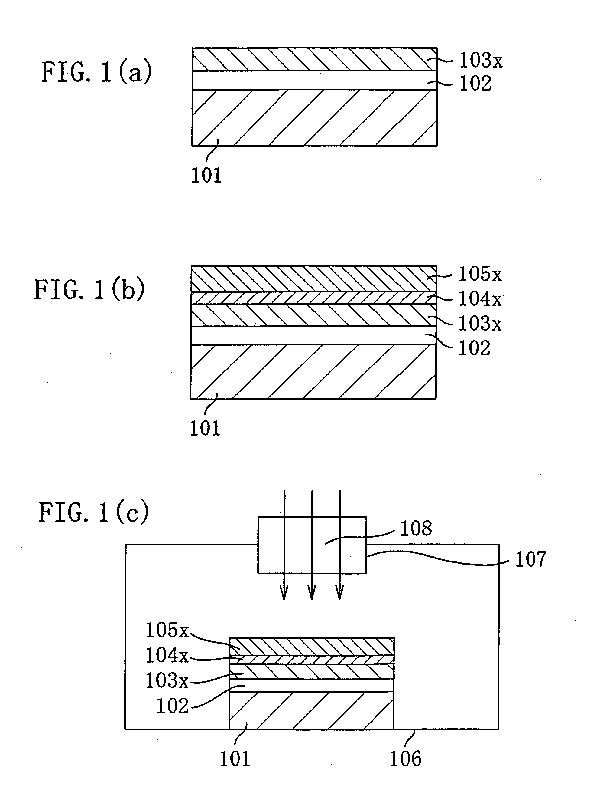
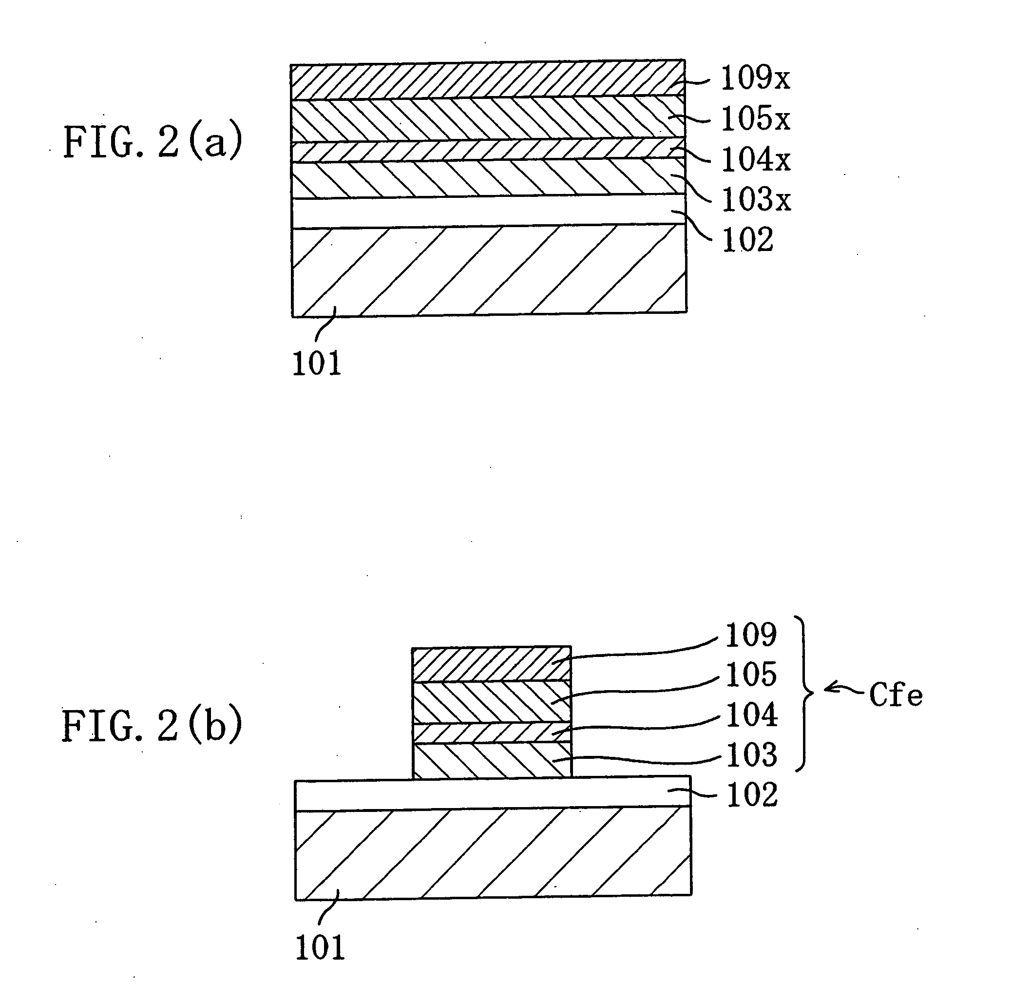
[0068] FIGS. 1(a) through 2(b) are cross-sectional views showing respective process steps for fabricating a semiconductor device according to a first embodiment of the present invention.
[0069] First, in a process step shown in FIG. 1(a), by thermal oxidation, for example, a silicon oxide film 102 with a thickness of 100 nm is formed on a p-type Si substrate 101, and then a Pt film 103x is deposited to a thickness of 200 nm over the silicon oxide film 102.
[0070] Next, in a process step shown in FIG. 1(b), with a sputtering process, a Ti film 104x is deposited to a thickness of 6 nm over the Pt film 103x, and then a ferroelectric PZT (Pb(Zr, Ti)O3) film 105x is deposited to a thickness of 500 nm at a substrate temperature of 600° C. In this case, the Pt film 103x serves as a lower electrode and the Ti film 104x serves as a seed layer for growing the PZT film 104x.
[0071] Then, in a process step shown in FIG. 1(c), the Si substrate 101 is placed inside a chamber 106, and an electroma...
embodiment 2
[0099] FIGS. 5(a) through 6(b) are cross-sectional views showing respective process steps for fabricating a semiconductor device according to a second embodiment of the present invention.
[0100] First, in a process step shown in FIG. 5(a), by thermal oxidation, for example, a silicon oxide film 202 with a thickness of 300 nm is formed on a p-type Si substrate 201, and then an Al film 203x is deposited to a thickness of 800 nm over the silicon oxide film 202.
[0101] Next, in a process step shown in FIG. 5(b), with a sputtering or CVD process, a SiO2 film 204x is deposited to a thickness of 10 nm over the Al film 203x, and then a ferroelectric PZT (Pb(Zr, Ti)O3) film 205x is deposited to a thickness of 300 nm at a substrate temperature of 600° C. During these process steps, the Si substrate 201 is kept at 400° C. or less.
[0102] Then, in a process step shown in FIG. 5(c), the Si substrate 201 is placed inside a chamber 206, and an electromagnetic wave in the frequency range from 10 GH...
embodiment 3
[0117] FIGS. 7(a) through 8(b) are cross-sectional views showing respective process steps for fabricating a semiconductor device according to a third embodiment of the present invention.
[0118] First, in a process step shown in FIG. 7(a), local oxidation of silicon, for example, is performed so that an isolation oxide film 302 with a thickness of about 400 nm having a so-called LOCOS structure is formed on part of a Si substrate 301. Then, to control the threshold voltage of the transistor, p-type dopant ions such as boron are implanted into the Si substrate 301. A channel stopper region doped with the p-type impurity such as boron is defined in part of the Si substrate 301 that is in contact with the isolation oxide film 302. In some cases, a p-well may be defined. Thereafter, the surface of the p-type Si substrate 301 is oxidized by thermal oxidation, thereby forming a gate oxide film 303 to be a gate insulating film having a thickness of about 10 nm on an active region surrounded...
PUM
 Abstract
Description
Claims
Application Information


