Twin waveguide based design for photonic integrated circuits

a photonic integrated circuit and waveguide technology, applied in the field of optical communication, can solve the problems of coupling to the passive waveguide, the relative inability to control the laing threshold current, and the waveguide coupling is strongly dependent on the device length, so as to reduce the coupling loss in the non-tapered atg structure, reduce the modal gain, and reduce the coupling loss

Inactive Publication Date: 2005-05-05
THE TRUSTEES FOR PRINCETON UNIV
View PDF8 Cites 17 Cited by
  • Summary
  • Abstract
  • Description
  • Claims
  • Application Information

AI Technical Summary

Benefits of technology

[0012] The invention provides an asymmetric twin waveguide (ATG) structure that significantly reduces the negative effects of modal interference and which can be effectively used to implement both lass and traveling-wave optical amplifiers (TWA). The ATG in the invention advantageously ensures stability in the laser and the TWA. In addition, the ATG provided in the invention can be monolithically fabricated on a single epitaxial structure without the necessity of epitaxial re-growth. Most importantly, the ATG, according to the present invention, is a versatile platform technology by which a variety of PICs, each with different layouts and components, can be fabricated from the same base wafer and modified with conventional semiconductor processing techniques to produce substantial modal gains and negligible coupling losses between PIC components.
[0013] In an embodiment of the ATG structure of the invention, the effective index of one of the passive waveguides in the ATG is varied from that of a symmetric twin waveguide such that one mode of the even and odd modes of propagation is primarily confined to the passive waveguide and the other to the active waveguide. As a result, the mode with the larger confinement factor in the active waveguide experiences higher gain and becomes dominant.
[0015] In a further embodiment, the active waveguide in a monolithically integrated device is laterally tapered by conventional semiconductor etching techniques. The tapered region of the active waveguide, at a junction of active and passive devices, helps to reduce coupling losses by resonant or adiabatic coupling of the optical energy between the passive waveguide and the active waveguide. As a result, the modal gain is significant compared to the symmetric TG structure and the coupling loss in the non-tapered ATG structure is reduced to negligible levels.

Problems solved by technology

The conventional TG structure, however, suffers from the disadvantage that waveguide coupling is strongly dependent on device length, due to interaction between optical modes.
A common problem in prior-art TG structure: is the relative inability to control the lasing threshold current and coupling to the passive waveguide as a consequence of the sensitivity to variations in the device structure itself.
This interaction leads to constructive and destructive interference in the laser cavity, which affects the threshold current, modal gain, coupling efficiency and output coupling parameters of the device.
In sum, the conventional TG structure suffers from unstable sensitivity in performance characteristics due to laser cavity length, even / odd mode interaction and variations in the layered structure.
However, the modified TG structure of the '866 patent is ineffective in a device with a traveling-wave optical amplifier (TWA), which is an important component in PICs designed for optical communication systems.
In a TG device with an absorption layer operated as a TWA, the additional absorption in the single pass through the active region is insufficient to remove the even mode.

Method used


Image

  • Twin waveguide based design for photonic integrated circuits
  • Twin waveguide based design for photonic integrated circuits
  • Twin waveguide based design for photonic integrated circuits

Examples


Embodiment Construction

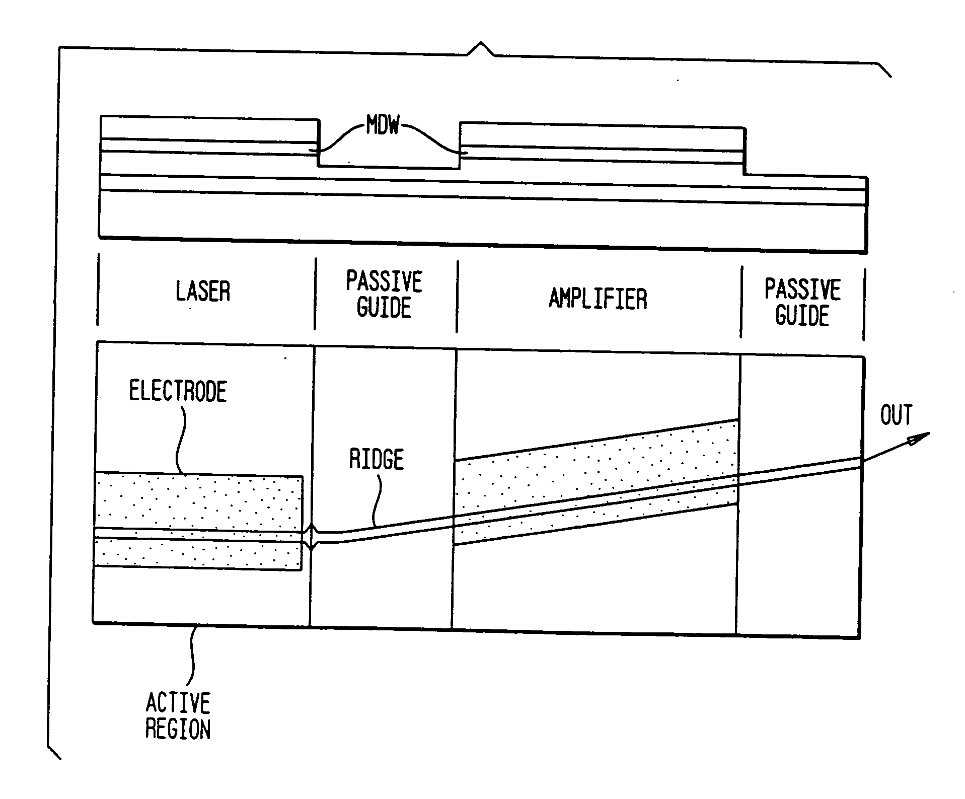
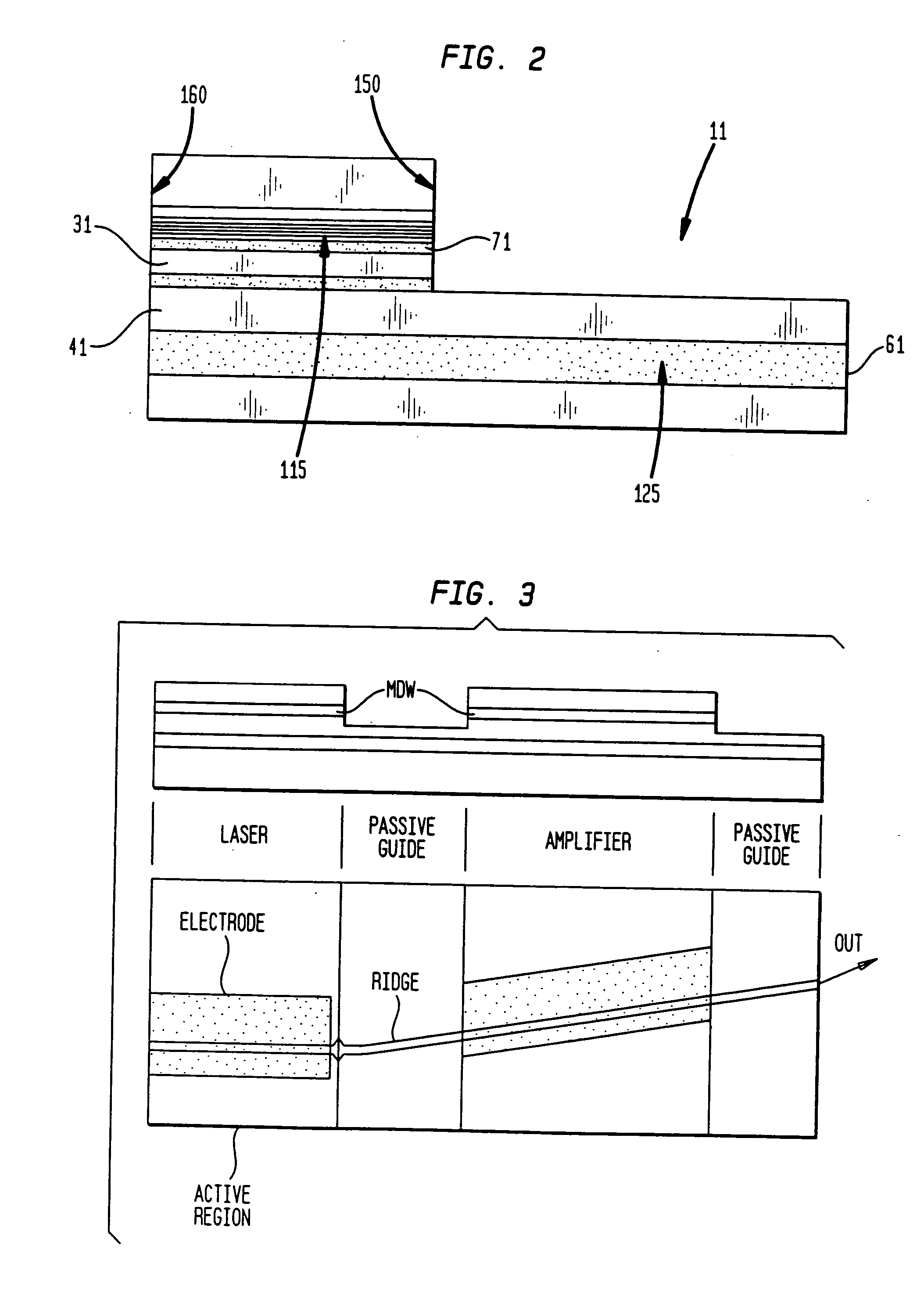
[0021] As already noted in the Background, the twin-waveguide approach to photonic integration represents a versatile platform technology by which a variety of PICs, each with different layouts and components, can be fabricated from the same base wafer—that wafer being grown in a single epitaxial growth step. Typically, the upper layer is used for active devices with gain (e.g., lasers SOAs), whereas the lower layer, with a larger bandgap energy, is used for on-chip manipulation of the optic energy generated by the active device(s) via etched waveguides. With such a TG structured PIC, active components such as semiconductor optical amplifiers (SOAs), Fabry-Perot and single frequency distributed Bragg reflector (DBR) lasers can be integrated with passive components such as Y-branches and multi-beam splitters, directional couplers, distributed Bragg feedback grating sections, multimode interference (MMI) couplers and Mach-Zehnder modulators.

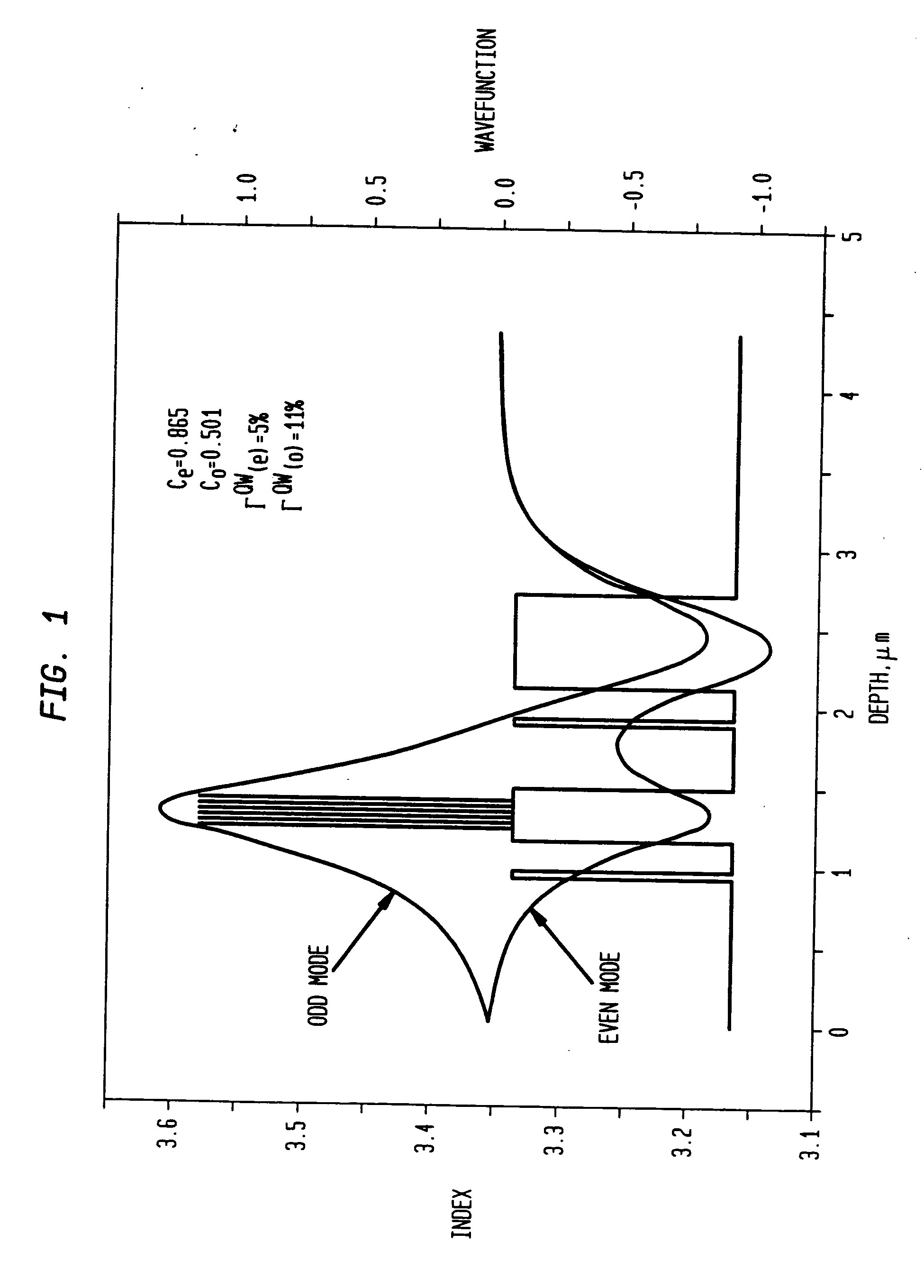
[0022] As previously noted, the simple TG s...


PUM

PropertyMeasurementUnit
angleaaaaaaaaaa
widthaaaaaaaaaa
energy gap cutoff wavelengthaaaaaaaaaa

Abstract

An asymmetric twin waveguide (ATG) structure is disclosed that significantly reduces the negative effects of inter-modal interference in symmetric twin-waveguide structures and which can be effectively used to implement a variety of optical devices. The ATG structure of the invention can be monolithically fabricated on a single epitaxial structure without the necessity of epitaxial re-growth. To achieve the ATG structure of the invention, the effective index of the passive waveguide in the ATG is varied from that of a symmetric twin waveguide such that one mode of the even and odd modes of propagation is primarily confined to the passive waveguide and the other to the active waveguide. The different effective indices of the two coupled waveguides result in the even and odd modes becoming highly asymmetric. As a result, the mode with the larger confinement factor in the active waveguide experiences higher gain and becomes dominant. In a further embodiment, the active waveguide is tapered to reduce coupling losses of the optical energy between the passive waveguide and the active waveguide. In a further embodiment, a grating region is incorporated atop the passive waveguide to select certain frequencies for transmission of light through the passive waveguide.

Description

RELATED APPLICATIONS [0001] The invention is related to U.S. Provisional Application 60 / 090,451, filed on Jun. 24, 1998, entitled TWIN WAVEGUIDE BASED DESIGN FOR PHOTONIC INTEGRATED CIRCUITS, the subject matter thereof being fully incorporated by reference hereinFIELD OF THE INVENTION [0002] The present invention is related to the field of optical communications, and more particularly to waveguide design in photonic integrated circuits. BACKGROUND OF THE INVENTION [0003] Photonic integrated circuits (PIC) provide an integrated technology platform increasingly used to form complex optical circuits. The PIC technology allows many optical devices both active and passive, to be integrated on a single substrate. For example, PICs may comprise integrated lase integrated receivers, waveguides, detectors, semiconductor optical amplifiers (SOA), and other active and passive optical devices. Such monolithic integration of active and passive devices in PICs provides an effective integrated tec...

Claims


Application Information

Patent Timeline
Patent Type & Authority Applications(United States)
IPC IPC(8): G02B6/122G02B6/12G02B6/28G02B6/34G02F1/01G02F1/295H01S5/026H01S5/10H01S5/34H01S5/50
CPCB82Y20/00G02B6/12004G02B6/12021G02B6/2813G02B2006/12121G02B2006/12178H01S5/50H01S5/1014H01S5/1032H01S5/1064H01S5/3403H01S5/34306G02B2006/12195
Inventor FORREST, STEPHEN R.GOKHALE, MILINDSTUDENKOV, PAVEL
Owner THE TRUSTEES FOR PRINCETON UNIV
Why Eureka
Try Eureka