High wireability microvia substrate

a microvia substrate and high wireability technology, applied in the direction of printed circuit aspects, printed circuit non-printed electric components, semiconductor/solid-state device details, etc., can solve the problems of increasing clock rates, compulsion to develop new manufacturing techniques, and complex integrated circuits with very high input/output (i/o) counts. achieve the effect of maintaining wireability density and reducing chip siz

Inactive Publication Date: 2005-05-19
IBM CORP
View PDF5 Cites 31 Cited by
  • Summary
  • Abstract
  • Description
  • Claims
  • Application Information

AI Technical Summary

Benefits of technology

[0008] One of the objects of the present invention is to permit a reduction in the chip size while maintaining wireability density.

Problems solved by technology

The development of increasingly complex integrated circuits with very high input / output (I / O) counts has been coupled with increasing clock rates to compel the development of new manufacturing techniques.
Initially, the C4 technology was limited to ceramic substrates due to the adverse effect that high temperatures required to reflow the tin solder on the chips had on the need to match the thermal expansion of the carrier substrate and that of the silicon chip.
However, with the development of low cost dielectrics such as FR-4 and standard reflow joining time / temperature profiles, this problem is no longer insurmountable.
Without the use of the encapsulant, the thermal cycle fatigue life of the joints would be unacceptable.
Without the ability to use some of these elements, the overall functionality of the system suffers.

Method used


Image

  • High wireability microvia substrate
  • High wireability microvia substrate
  • High wireability microvia substrate

Examples


Embodiment Construction

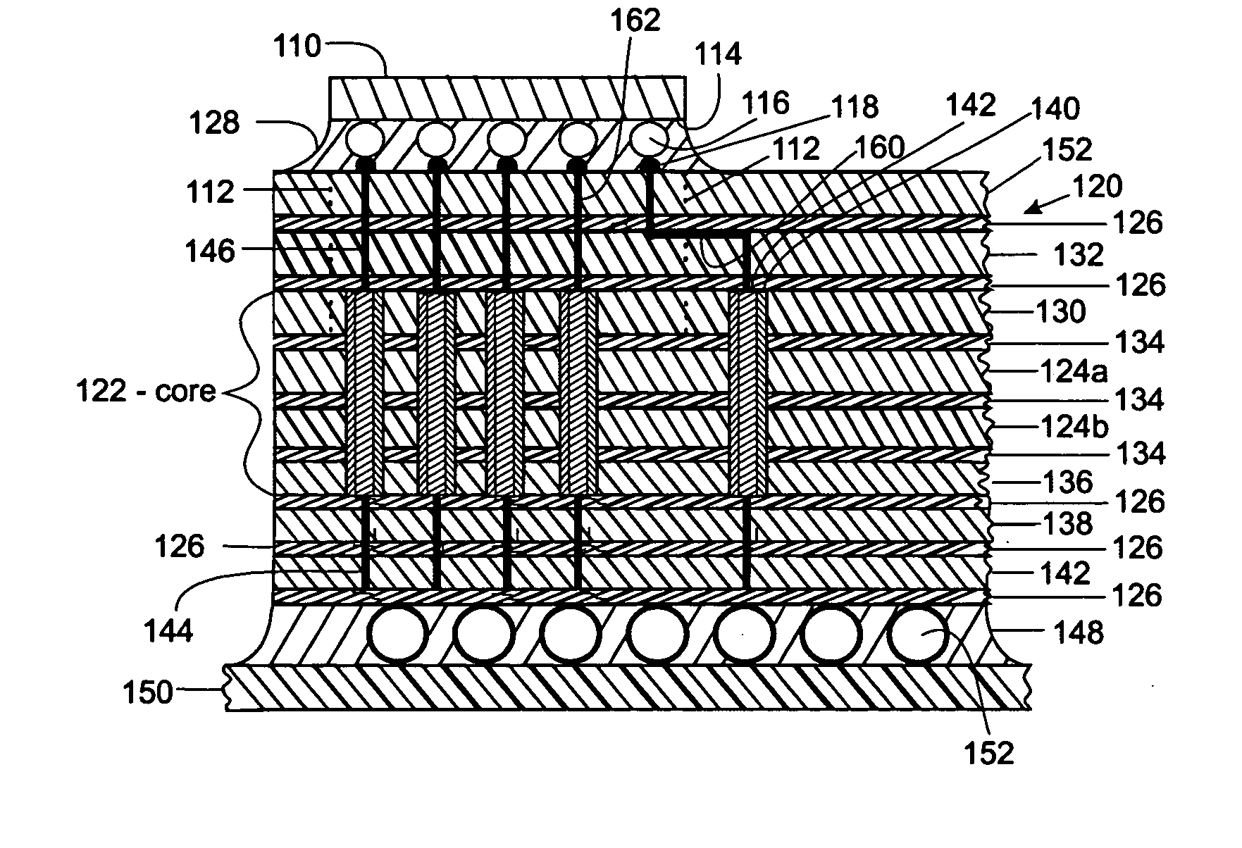
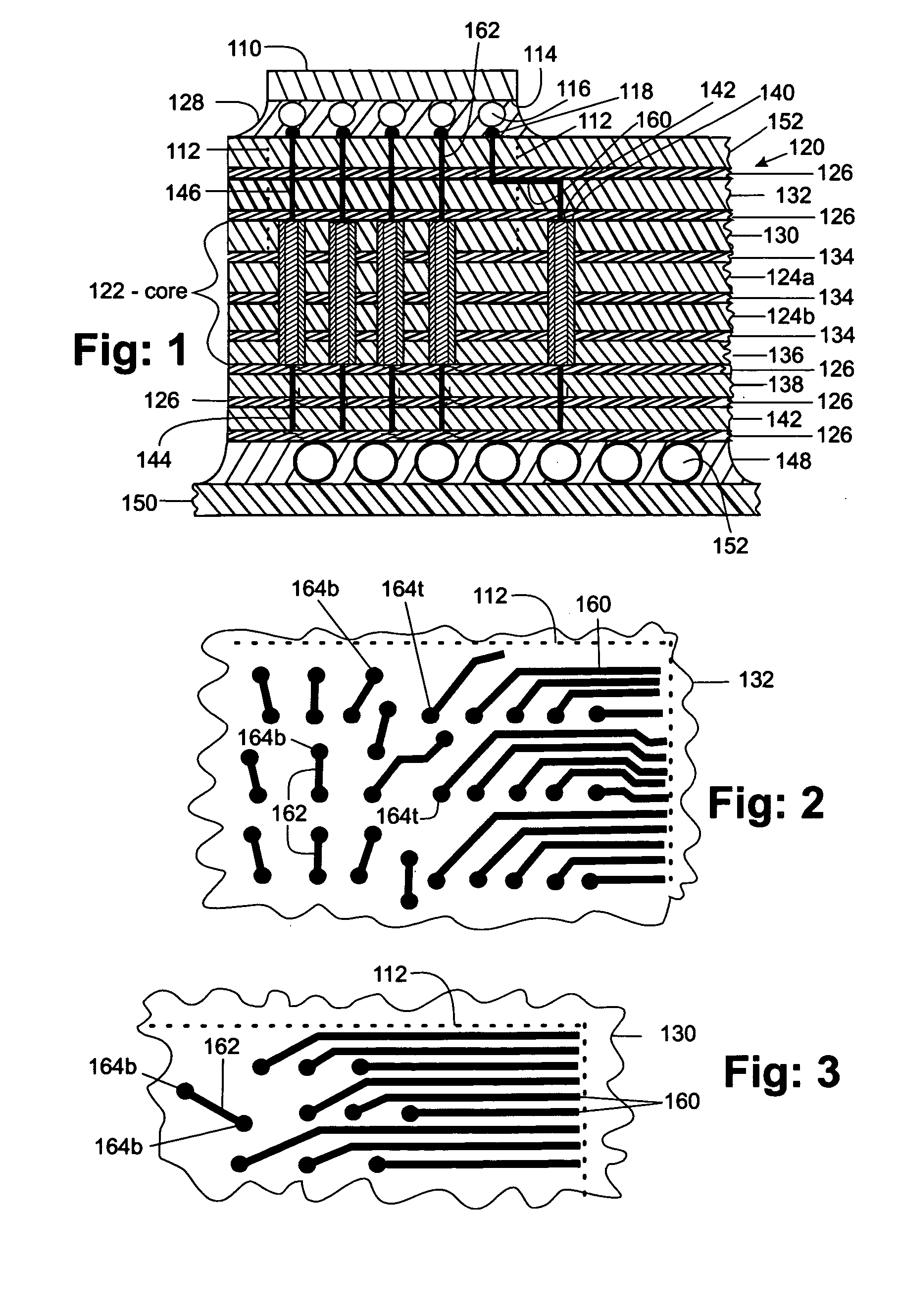
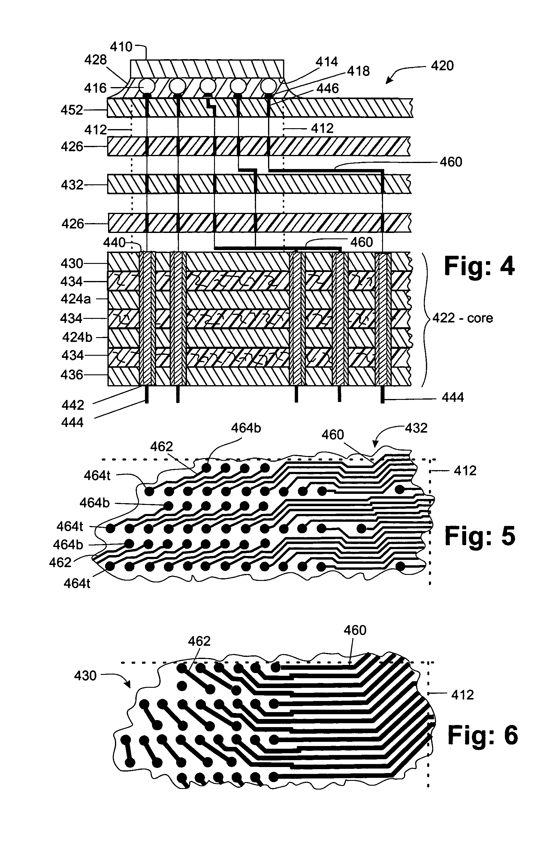
[0021] A chip is typically made from a material such as silicon which exhibits semiconductive properties. The chip is mounted on a carrier which in turn is mounted on a printed wiring board. The carrier contains a large number of small conductive pathways, which for purposes of the present invention are referred to as vias passing through the core and microvias passing through the remainder of the carrier for tnansmitting signals between the chip and the printed wiring board. The carrier contains a core and one or more signal planes above and below the core. The core contains one or more voltage / ground planes as dictated by power consumption requirements, the planes separated from one another by a reinforced dielectric material. One conductive signal layer of copper forms the top of the core and is labeled as FC-1. A second conductive layer forms a second signal layer located above the core and is labeled as FC-2. If additional signal layers are used on the top of the core, they are...


PUM


Abstract

The escape of signals from a semiconductor chip to a printed wiring board in a flip chip/ball grid array assembly is improved by repositioning the signals from the chip through the upper signal layers of the carrier. This involves fanning out the circuit lines through the chip carrier from the top surface that communicates with the chip, through the core to the bottom surface where signals exit the carrier to the printed wiring board. This fanning out is achieved by making better utilization of the surface area of the signal planes between the core and the chip. The signals are fanned out on each of the top signal planes so that many more of the signals are transmitted through the vias in the core to the bottom signal planes where they can escape outside of the footprint area of the chip thereby increasing the density of circuits escaping the footprint area.

Description

FIELD OF THE INVENTION [0001] This invention relates to increasing the density of the signal output from a semiconductor microchip through a chip carrier to a printed wiring board for use in such applications as computers and telecommunication devices. More particularly, the invention relates to the application of this technology to flip chip-ball grid array packaging. BACKGROUND OF THE INVENTION [0002] The development of increasingly complex integrated circuits with very high input / output (I / O) counts has been coupled with increasing clock rates to compel the development of new manufacturing techniques. In addition, the number of electronic devices that require portability is constantly growing, thereby compelling reductions in system size and weight without adversely affecting reliability. Further adding to this is the advent of the broadband which has greatly increased the requirements for signal transmission in integrated devices and their packaging. Because of these trends, pri...

Claims


Application Information

Patent Timeline
Patent Type & Authority Applications(United States)
IPC IPC(8): H05K1/18H01L23/12H01L23/498H05K1/11H05K3/46
CPCH01L23/49822H01L2224/16235H01L23/49833H01L2224/16H01L2924/01078H01L2924/09701H01L2924/15173H01L2924/15174H01L2924/15311H01L2924/15312H05K1/112H05K2201/09227H05K2201/10674H01L2924/01019H01L2924/01087H01L2924/01322H01L2224/16225H01L2224/32225H01L2224/73204H01L23/49827H01L2924/10253H01L2924/00H05K1/11
Inventor MEMIS, IRVING
Owner IBM CORP
Why Eureka
Try Eureka