Thin film multilayer body, electronic device and actuator using the thin film multilayer body, and method of manufacturing the actuator

Inactive Publication Date: 2005-05-19
FUJITSU LTD
View PDF6 Cites 23 Cited by
  • Summary
  • Abstract
  • Description
  • Claims
  • Application Information

AI Technical Summary

Benefits of technology

[0032] According to the present invention, the oxide layer of a crystalline structure having a simple perovskite lattice is epitaxially grown and formed. Accordingly, the oxide layer has good crystallinity, and therefore, shows a good piezoelectric or electrostrictive property. Further, since the silicon or gallium arsenide single crystal substrate is employed, it is possible to increase area and reduce cost compared with the case of employing the conventional MgO single crystal substrate.
[0033] The process of forming an amorphous layer between the single crystal substrate and the intermediate layer by heat treatment may

Problems solved by technology

Of piezoelectric and electrostrictive materials, those showing a practically sufficient piezoelectric or electrostrictive property are limited to some oxides.
In particular, materials that have perovskite structures and show good properties are limited to oxides.
In general, however, it is not easy to obtain a single crystal film.
However, commonly used oxide single crystal substrates are approximately 2 in., and are difficult to increase in size.
Further, in terms of price, while 6 in. silicon single crystal substrates cost several thousand yen, 2 in.
Mg

Method used


Image

  • Thin film multilayer body, electronic device and actuator using the thin film multilayer body, and method of manufacturing the actuator
  • Thin film multilayer body, electronic device and actuator using the thin film multilayer body, and method of manufacturing the actuator
  • Thin film multilayer body, electronic device and actuator using the thin film multilayer body, and method of manufacturing the actuator

Examples


first embodiment

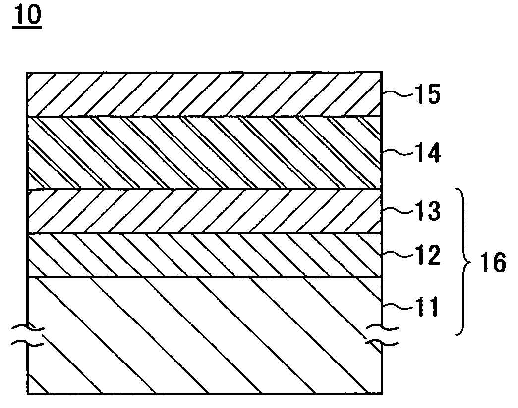
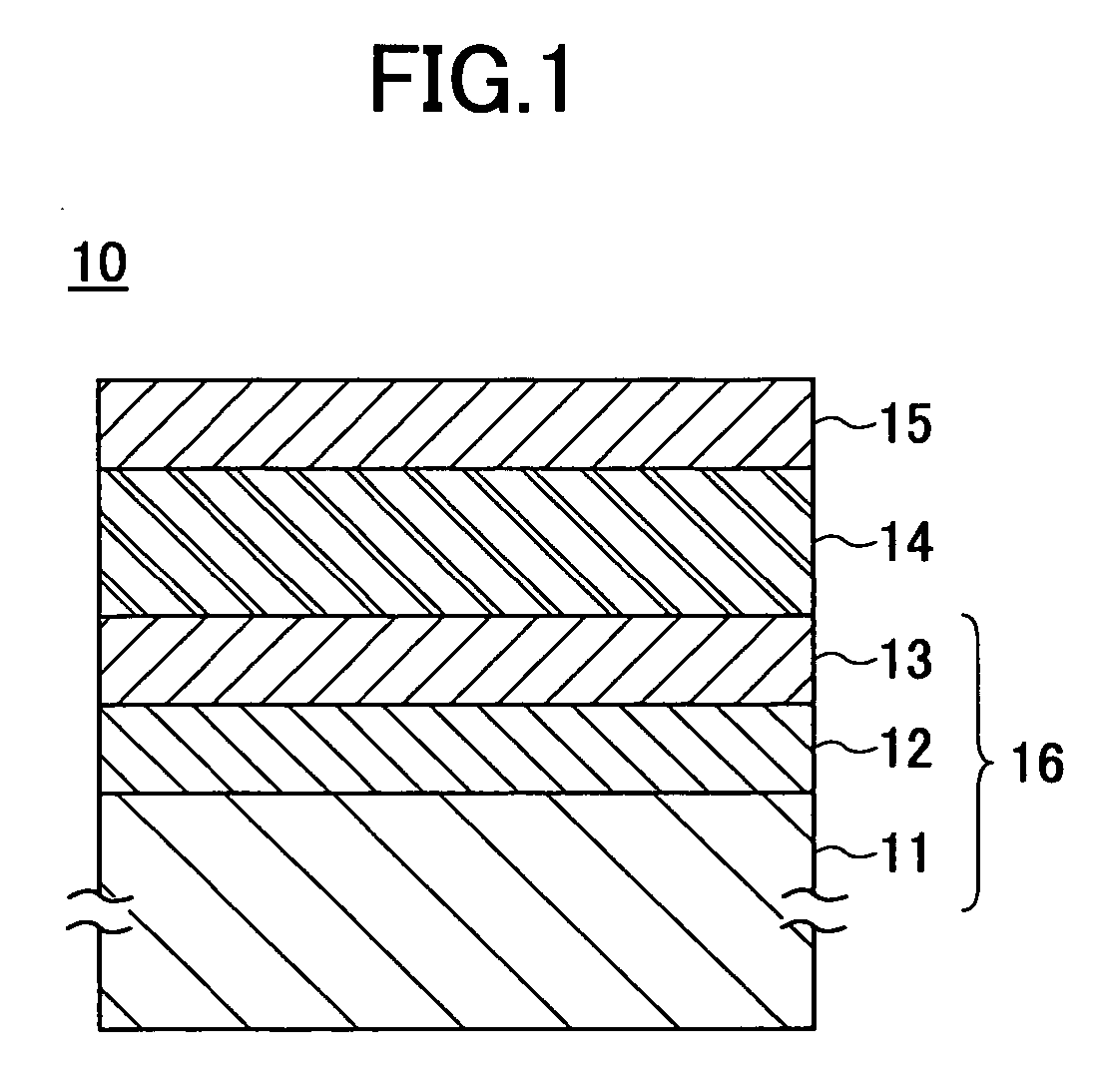
[0081] A description is given below of an actuator according to an embodiment according to this mode of implementation. According to the actuator of this embodiment, magnesia spinel, a platinum film that is a lower conductive layer (electrode), a PZT film as an oxide layer, and an upper conductive layer are stacked sequentially on a silicon single crystal substrate.

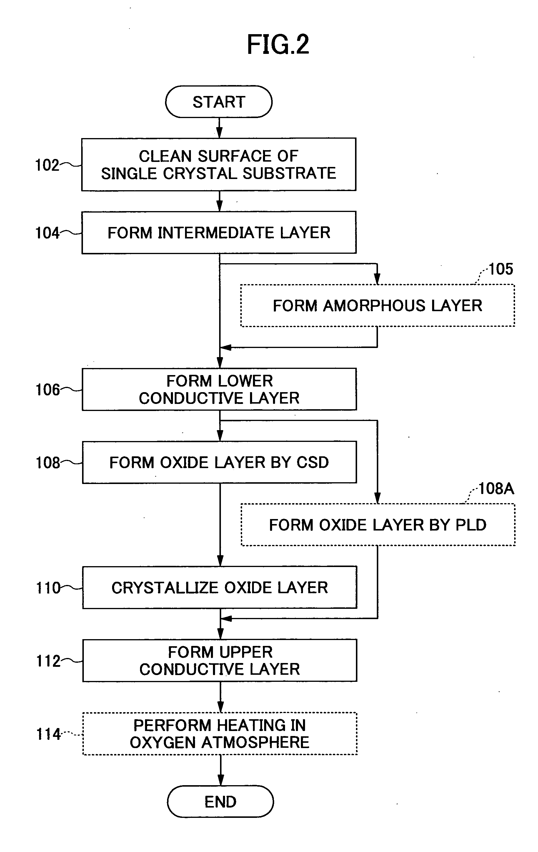
[0082] First, a 2 in. silicon single crystal substrate whose principal plane is the (001) surface was cleaned, and thereafter, was soaked in a 9 wt. % dilute hydrofluoric acid so that a natural oxide film (SiOx) was removed from the surface of the silicon single crystal substrate.

[0083] Next, magnesia spinel of 100 nm in thickness is formed on the silicon single crystal substrate by CVD. Specifically, the silicon single crystal substrate was disposed in a CVD film formation chamber, and maintained at a substrate temperature of 900° C. MgCl2 was employed as a Mg material. It was heated to 500° C. in a Mg source chamber t...

second embodiment

[0089] An actuator according to this embodiment is the same as in the first embodiment except that an iridium film is formed instead of the platinum film of the lower conductive layer and that PLZT is employed for the oxide layer of the first embodiment. In the following, a description of the same manufacturing processes as in the first embodiment is omitted.

[0090] According to the actuator of this embodiment, magnesia spinel, an iridium film that is a lower conductive layer, a PLZT film as an oxide layer, and an upper conductive layer are stacked sequentially on a silicon single crystal substrate.

[0091] The iridium film was formed to be 200 nm in thickness on the magnesia spinel film by sputtering. Specifically, the pressure inside a sputtering device was set to 1 Pa (7.5×10⁻³ Torr), and while letting 30 sccm of argon gas and 1 sccm of oxygen gas flowing, the substrate was heated to 600° C. so as to cause its epitaxial growth.

[0092] The PLZT film was formed on the iridium film b...

third embodiment

[0100] An actuator according to this embodiment is the case of providing a thermal oxide layer between the silicon single crystal substrate and the intermediate layer of the first embodiment, and is the same as in the first embodiment except that the thermal oxide layer is provided and that the oxide layer is formed by PLD.

[0101] The actuator of this embodiment is formed by sequentially stacking a thermal oxide layer, a magnesia spinel film, an iridium film, a PZT film, and a platinum film on a silicon substrate.

[0102] The thermal oxide layer is formed in an oxygen atmosphere with a furnace after forming the magnesia spinel on the silicon substrate. Specifically, heating is performed at 1050° C. for two hours while letting vapor flowing to the furnace at 10 L / min. by bubbling using oxygen gas as a carrier gas. The thermal oxide layer of 150 nm in thickness was formed.

[0103] Next, the PZT film was formed by PLD. Specifically, using a target of PNN-PT-PZ50 / 35 / 15 including 30 mol % ...


PUM

PropertyMeasurementUnit
Electrical conductivityaaaaaaaaaa
Structureaaaaaaaaaa
Electrical conductoraaaaaaaaaa

Abstract

A thin film multilayer body is disclosed that includes a single crystal substrate of silicon or gallium arsenide; an intermediate layer of magnesia spinel formed on the single crystal substrate by epitaxial growth; and a conductive layer of a platinum-group element formed on the intermediate layer by epitaxial growth. An oxide layer is to be epitaxially grown on the conductive layer, the oxide layer having a crystalline structure having a simple perovskite lattice.

Description

CROSS REFERENCE TO RELATED APPLICATION [0001] This application is a U.S. continuation application filed under 35 USC 111(a) claiming benefit under 35 USC 120 and 365(c) of PCT International Application No. PCT / JP03 / 13500, filed Oct. 22, 2003, which claims priority to Japanese Patent Application No. 2002-324363, filed on Nov. 7, 2002. The foregoing applications are hereby incorporated by reference.BACKGROUND OF THE INVENTION [0002] 1. Field of the Invention [0003] The present invention relates to a thin film multilayer body in which an oxide layer that has a crystalline structure having a simple perovskite lattice in the crystal and shows a high dielectric property, a piezoelectric property, a ferroelectric property, a pyroelectric property, etc., can be grown epitaxially; a thin film multilayer body in which such an oxide layer is formed; and an electronic device having the thin film multilayer body in which such an oxide layer is formed. The electronic device is suitable for, for i...

Claims


Application Information

Patent Timeline
IPC IPC(8): C23C16/40C30B29/26G02F1/1339H01L21/8246H01L27/105H01L41/08H01L41/09H01L41/18H01L41/187H01L41/22H01L41/29H01L41/317H01L41/39
CPCH01L41/1875H01L41/0815H01L41/319H01L41/29H10N30/10516H10N30/8548H10N30/079H10N30/06H10N30/00
Inventor KONDO, MASAOYAMAWAKI, HIDEKI
Owner FUJITSU LTD
Why Eureka
Try Eureka