Lithographic mask, and method for covering a mask layer

a mask and mask layer technology, applied in the field of lithographic masks, can solve the problems of reducing the size of the structure imaged on the exposed semiconductor wafer, affecting and fabricated defects, so as to ensure the quality of optical imaging and prevent the impurity particles. , the effect of high quality

Inactive Publication Date: 2005-05-19
POLARIS INNOVATIONS
View PDF4 Cites 7 Cited by
  • Summary
  • Abstract
  • Description
  • Claims
  • Application Information

AI Technical Summary

Benefits of technology

[0010] In one aspect, the present invention provides an inexpensive mask and an inexpensive method for producing it in which impurities caused by impurity particles are reliably prevented and at the same time a high quality of the optical imaging is ensured.

Problems solved by technology

Over the course of time, impurity particles and other impurities may be deposited on the mask, having an adverse effect on the quality of the optical imaging and leading to defects on the structure which is imaged on a reduced scale onto the exposed semiconductor wafers.
This produces defects in the semiconductor circuits, which are fabricated.
To avoid such defects, it is true that it is possible for a mask to be cleaned at relatively long intervals, but this operation is complex and increases production costs.
Therefore, even when a pellicle is fitted, contact with the clean-room air is possible via the openings in the pellicle frame, and over the course of time this leads to contamination to the patterned mask layer.
These contaminations, for example caused by ammonium sulfide, amines, sulfur oxides or impurity particles, are present in trace amounts even in clean-room air and, once they have penetrated between the pellicle and the mask layer, cannot be removed again without complex cleaning.
On the other hand, completely closing up the pellicle frame would no longer allow pressure compensation.
However, the production of continuously dense protective layers involves more time and labor, since their surface, which is remote from the mask layer, has to be planarized at considerable cost in order not to adversely affect the quality of the optical imaging.

Method used


Image

  • Lithographic mask, and method for covering a mask layer
  • Lithographic mask, and method for covering a mask layer
  • Lithographic mask, and method for covering a mask layer

Examples


Embodiment Construction

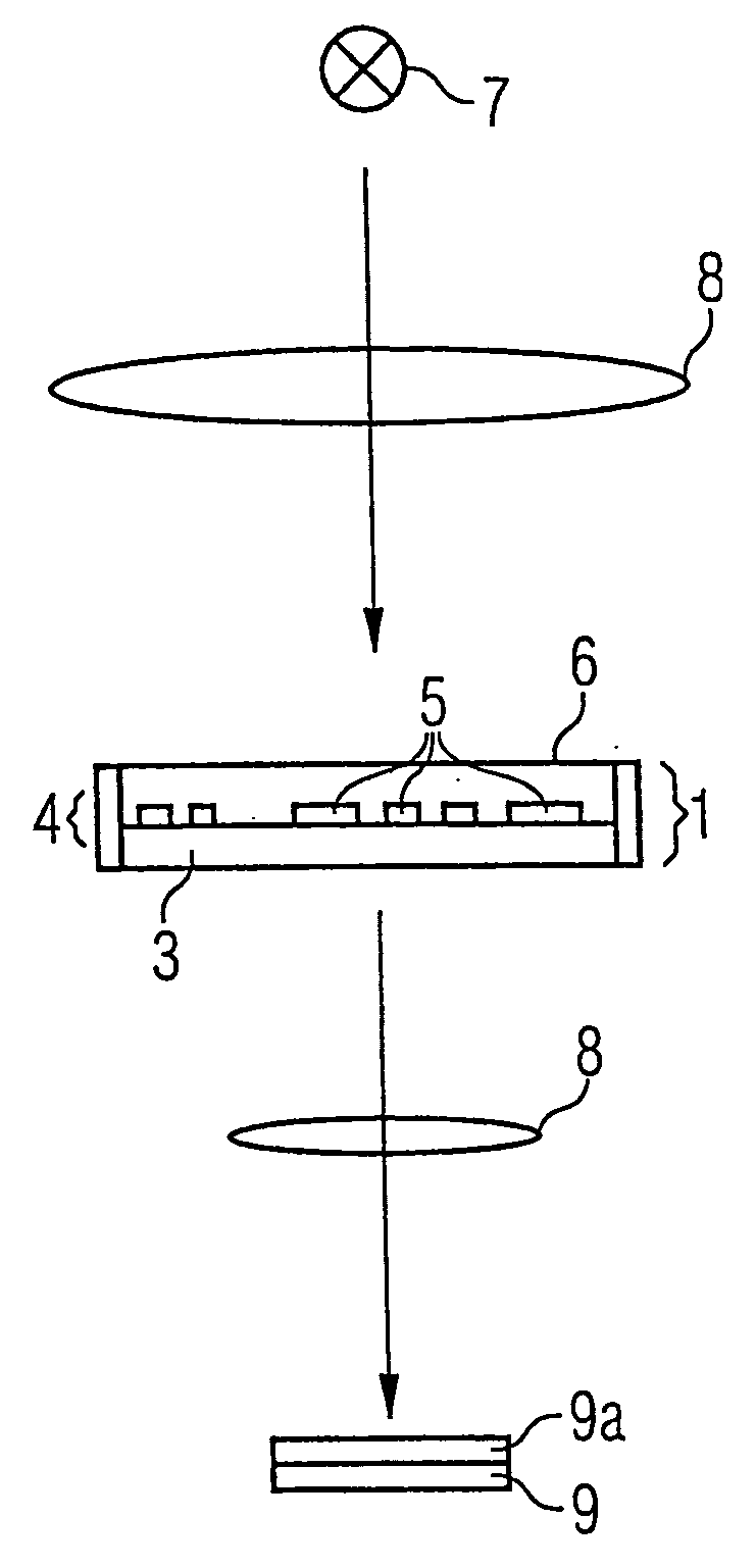
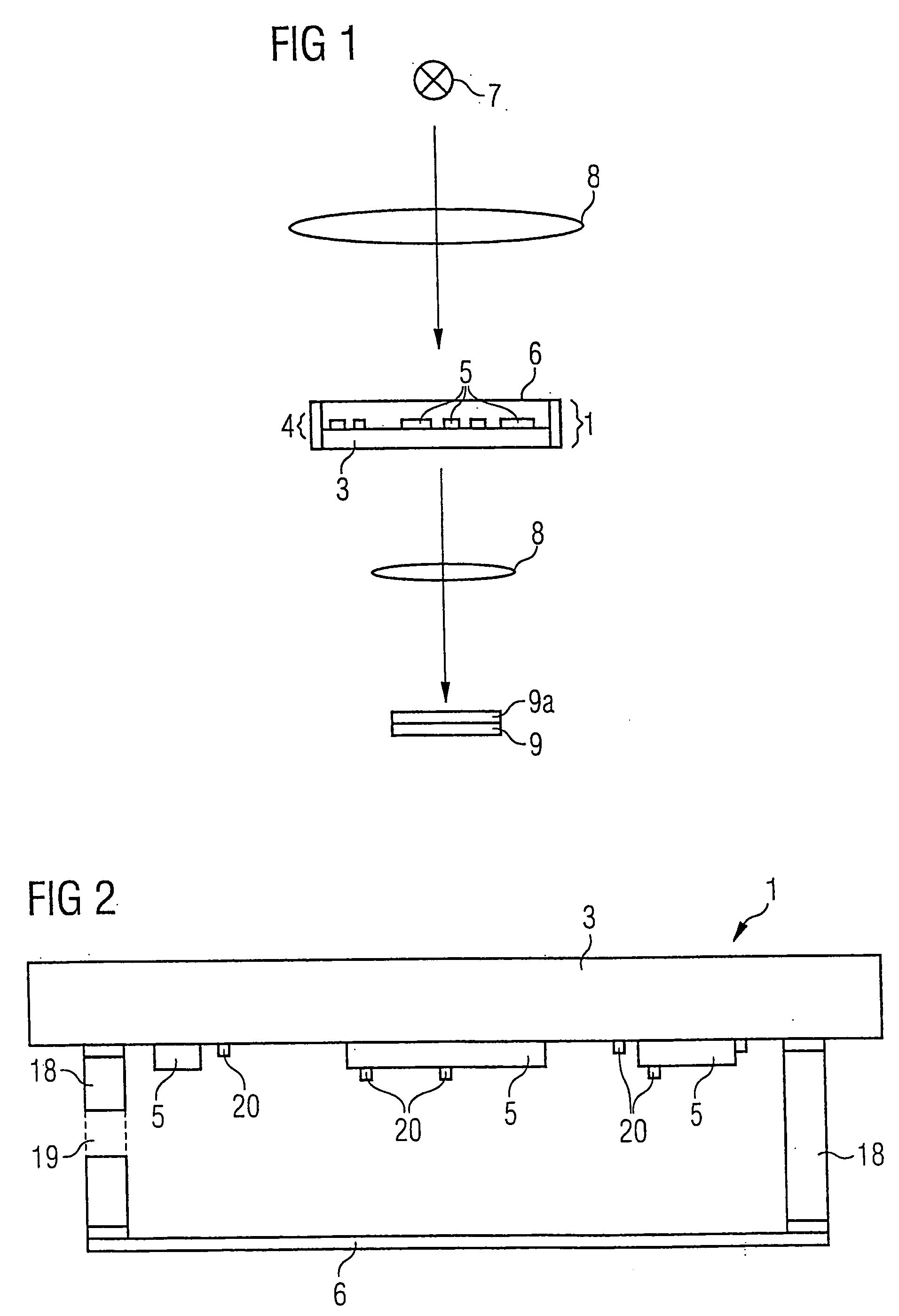
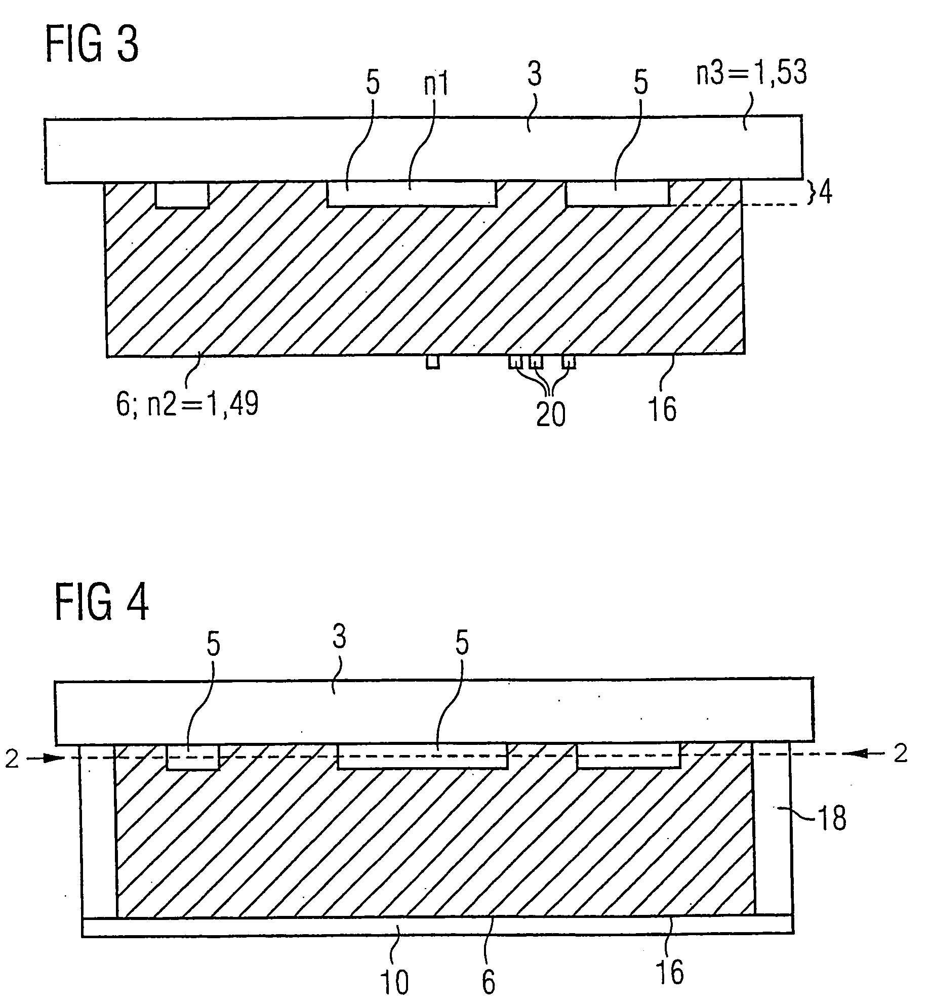
[0050] Preferred embodiments of the invention will now be described with the figures. Referring first to in FIG. 1 electromagnetic radiation from a light source 7 passes through an optical system 8 and through a mask 1 onto a substrate 9, which is to be exposed by lithography or onto a layer 9a, which is to be exposed on the substrate 9. The system is used to transfer a structure of the mask 1 onto the substrate 9. Regions of the exposed substrate, which correspond to the structures 5 of the patterned mask layer 6 are shadowed and can be removed or retained selectively with respect to exposed regions. As an alternative to the case of a transmission mask illustrated in FIG. 1, the mask 1 may also be a reflection mask. In both cases, the mask substrate 3 prevents impurity particles from forming or being deposited from just one side. From the other side, it is customary to provide a pellicle, which is held as a protective layer 6 at a distance from the patterned mask layer 4 and preven...


PUM

PropertyMeasurementUnit
refractive indexaaaaaaaaaa

Abstract

A lithographic mask having a mask substrate (3) and a patterned mask layer (4) which includes mask structures (5) and can be transferred by lithography to a further substrate is disclosed. With masks of this type, it is customary for a protective layer to be provided in the form of a membrane positioned at a distance from the mask layer (4), in order to keep impurity particles or other impurities away from the focal plane of the mask layer (4). According to the invention, the protective layer (6) is applied in liquid form directly to the mask structures (5) and fills up spaces between the mask structures (4). Then, the protective layer (6), while it is still in the liquid state, is covered with a plane-parallel plate. The continuously dense protective layer (6) which is formed in accordance with the invention is even more reliable in preventing impurity particles or impurities (20) from penetrating into spacers between the structures (5) of the mask layer (4). The impurity particles or impurities (20) can only be deposited on the outer side (16) of the protective layer (6), at a still greater distance from the focal plane.

Description

[0001] This application claims priority to German Patent Application 103 45 476.4, which was filed Sep. 30, 2003, and is incorporated herein by reference. TECHNICAL FIELD [0002] The invention relates to a lithographic mask having a mask substrate and having a patterned mask layer, which is arranged on one side of the mask substrate and includes mask structures. The invention also relates to a method for covering a patterned mask layer, which includes mask structures and can be transferred by lithography, of a mask with a protective layer. BACKGROUND [0003] Lithographic masks (reticles) are used in semiconductor fabrication to transfer structure patterns, which are formed thereon, of a ready-patterned mask layer onto a substrate, in particular a semiconductor substrate or a wafer, on a reduced scale with the aid of lithographic exposure. Regions of the substrate that correspond to the transmissive mask regions are exposed and can be patterned, etched or exposed to ion implantations a...

Claims


Application Information

Patent Timeline
Patent Type & Authority Applications(United States)
IPC IPC(8): A47G1/12B44F1/00G03C5/00G03F1/48G03F1/62G03F9/00G21K5/00H01L21/8238
CPCG03F1/62G03F1/48
Inventor SCHROEDER, UWE PAULBROERMANN, OLIVER
Owner POLARIS INNOVATIONS
Why Eureka
Try Eureka