Formation of high-mobility silicon-germanium structures by low-energy plasma enhanced chemical vapor deposition

a technology of low-energy plasma and chemical vapor deposition, which is applied in the direction of crystal growth process, coating, chemistry apparatus and processes, etc., can solve the problems of low growth rate, difficult fabrication of ge-rich sige structures and devices, and high unfavorable industrial mass production, and achieves a dramatic increase in growth rate

Inactive Publication Date: 2005-06-02
DICHROIC CELL
View PDF0 Cites 11 Cited by
  • Summary
  • Abstract
  • Description
  • Claims
  • Application Information

AI Technical Summary

Benefits of technology

[0035] It is an advantage of the invention presented herein, that the obstacles and disadvantages of known approaches can be circumvented or even avoided. Devices can be realized with hitherto unknown hole mobility. The growth rate was drastically increased thus allowing the inventive process to be used for Industrial manufacturing of semiconductor devices. Further advantages become obvious from the detailed description.

Problems solved by technology

Using these processes the fabrication of Ge-rich SiGe structures and devices is difficult.
It is another disadvantage of the known approaches that the growth rate is low.
This is, however, highly unfavorable for Industrial mass production.
The hot-wall UHV-CVD has several disadvantages, such as low growth rate on the order of about nm / min at substrate temperatures around 550° C. for pure Si, as reported by B. S. Meyerson et al. in “Cooperative growth phenomena in silicon / germanium low-temperature epitaxy”, Appl. Phys. Lett., Vol. 53, p.
The surface roughness has a detrimental effect on the quality of MODFETs, as described by M. Arafa et al. in “Device and fabrication issues of high performance Si / SiGe Fets”, Nat. Sci. Soc., Symp. Proc. Vol. 533, p.
The hot-wall process is thus not suited for high mobility hole transport.
High performance p-MODFETs with pure Ge channels thus cannot be made using the hot-wall technique.
Heterostructure devices cannot be formed on these rough surfaces without applying a chemical-mechanical polishing (CMP) process.
943, 1998, the relatively high process temperatures in an LPCVD process also lead to a remarkable surface roughness.
LPCVD, like cold-wall UHV-CVD, Is not suited for making structures that require a high hole mobility.
The most serious disadvantage of MBE is the limited capacity of the evaporation crucibles.
This is a disadvantage in particular when growing thick SiGe-buffer layers, as described by T. Hackbarth et al. in “Alternatives to thick MBE-grown relaxed SiGe buffers”, Thin Solid Films, Vol. 369, p.
MBE is thus not well suited for an industrial production of SiGe devices.
In particular pure Ge-layers show a remarkable surface roughness, except when the layers are grown at low substrate temperature around 300° C. At such low temperatures, however, the electrical properties of the devices are not acceptable anymore.

Method used


Image

  • Formation of high-mobility silicon-germanium structures by low-energy plasma enhanced chemical vapor deposition
  • Formation of high-mobility silicon-germanium structures by low-energy plasma enhanced chemical vapor deposition
  • Formation of high-mobility silicon-germanium structures by low-energy plasma enhanced chemical vapor deposition

Examples


Embodiment Construction

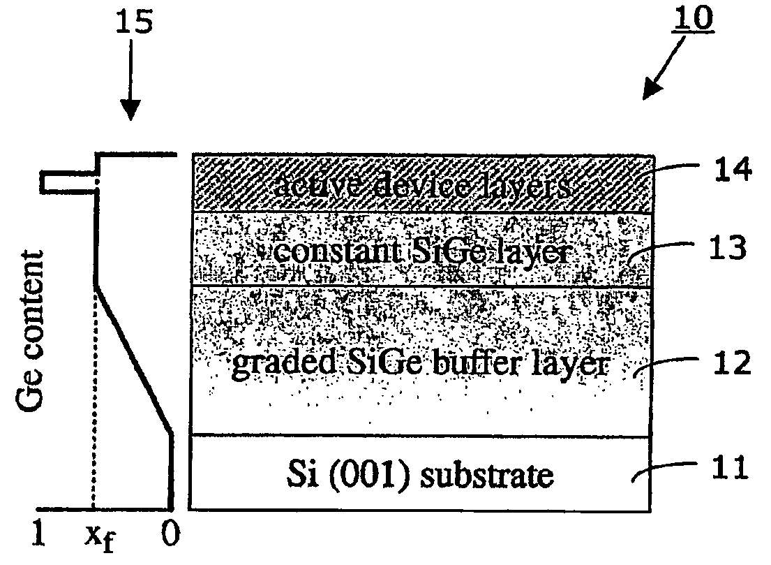
[0045] The present invention takes advantage of the principle of strained layer epitaxy when two materials with different lattice parameters are grown on top of one another. When germanium (Ge), for example, is deposited on top of a substrate with a smaller lattice parameter, the Ge atoms line up with the atoms underneath, compressively straining the Ge. In the strained Ge, for example the holes experience less resistance and have the ability to flow faster. This effect can be used to realize devices that are faster without having to shrink the size of the individual devices.

[0046] The silicon has slightly smaller spaces between the atoms than the germanium crystal lattice. A SiGe-layer thus has a lattice constant that is larger than the lattice constant of silicon. The lattice constant of SiGe increases with increasing concentration of the Ge.

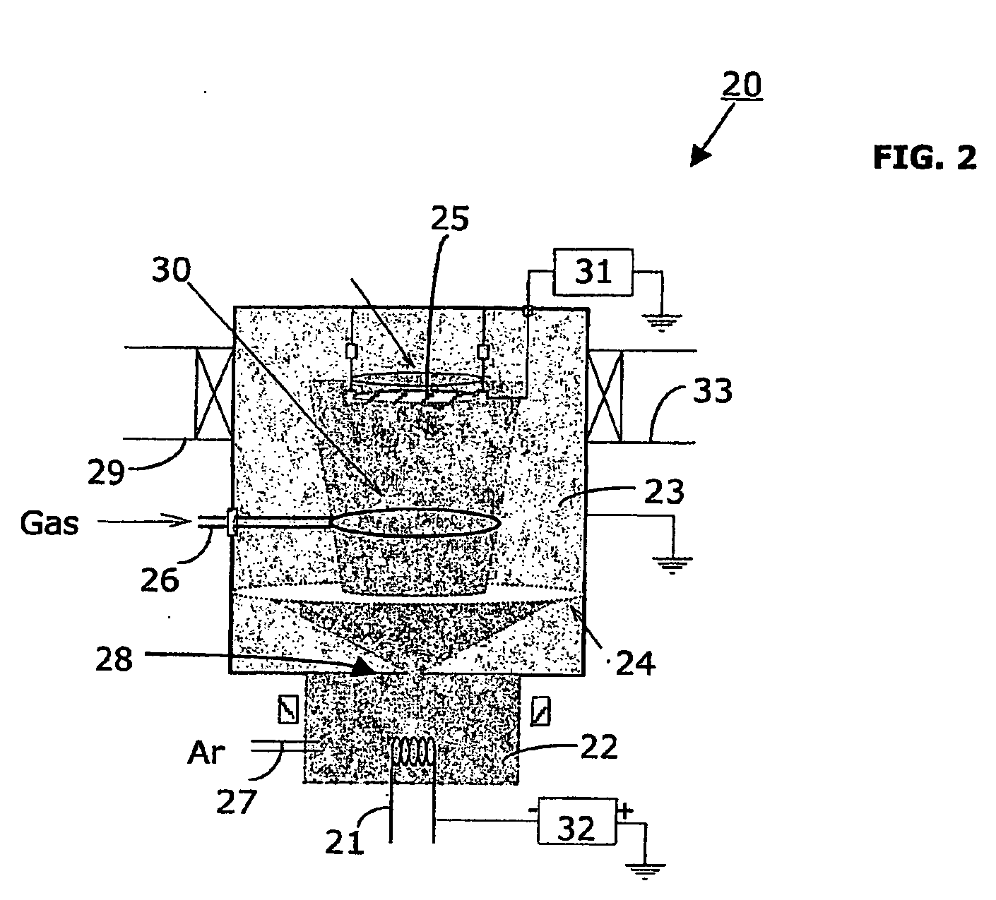
[0047] The present invention relies on low-energy plasma enhanced chemical vapor deposition (LEPECD). A typical LEPECVD system 20 is depict...


PUM

PropertyMeasurementUnit
temperatureaaaaaaaaaa

Abstract

A method for making a semiconductor heterostructure in a growth chamber with gas inlet comprises several steps. In a first step, a virtual substrate is formed on a silicon substrate, comprising a graded Si1-xGex layer followed by a Si1-xGex layer with constant concentration of Ge, using a high-density, low-energy plasma enhanced chemical vapor deposition (LEPECVD) process. In this step, the growth rate is maintained above 2 nm/s. the substrate temperature between 400° and 850° C., and the total reactive gas flow at the gas inlet between 5 sccm and 200 sccm. In another step, an active region is formed on said virtual substrate comprising a Ge-channel and a modulation-doped layer using a low-density, low-energy plasma enhanced chemical vapor deposition (LEPECVD) process. In this step, hydrogen (H2) is introduced into the growth chamber to act as a surfactant, a substrate temperature is maintained between 400° and 500° C. and a dopant gas is introduced in a pulsed manner into the growth chamber to provide for the modulation-doped layer.

Description

[0001] The present invention concerns the formation of silicon-germanium structures, in particular heterostructures, showing a drastically increased hole mobility. Modulation-doped field-effect transistor structures (e.g., MODFET structures) and modulation-doped quantum well structures (e.g., MODQW structures), for instance, can be made using the process presented hereinafter. BACKGROUND OF THE INVENTION [0002] New materials and material compositions are being employed in industry in order to Improve semiconductor devices such as transistors, for example. This allows to Improve the processing speed and performance of integrated circuits (ICs). [0003] A typical example is the deployment of Silicon-Germanium (SiGe) on Silicon. An example of a well-known SiGe heterostructure device 10 is illustrated in FIG. 1. The device 10 comprises a (001)-oriented silicon substrate 11. A graded SiGe-layer 12 is situated on top of the Si substrate 11. The layer 12 allows for a gradual modification of...

Claims


Application Information

Patent Timeline
Patent Type & Authority Applications(United States)
IPC IPC(8): C23C16/50H01L21/205H01L21/338H01L29/778H01L29/812
CPCH01L29/7782H01L21/0251H01L21/02381H01L21/0262H01L21/02502H01L21/02532H01L21/0245
Inventor VON KANEL, HANS
Owner DICHROIC CELL
Why Eureka
Try Eureka