Metallic compound thin film and method of fabricating the same, semiconductor device including metallic compound thin film and method of fabricating the device

a technology of metallic compound and thin film, which is applied in the direction of semiconductor devices, basic electric elements, electrical equipment, etc., can solve the problems of limited benefits of restricting the penetration of elements such as boron in the gate electrode, and no solution is provided to the problem, and achieves high insulation

Inactive Publication Date: 2005-06-02
ROHM CO LTD
View PDF5 Cites 11 Cited by
  • Summary
  • Abstract
  • Description
  • Claims
  • Application Information

AI Technical Summary

Benefits of technology

[0010] The first annealing in an atmosphere including a nitrogen compound gas diffuses nitrogen in a metal oxide film and forms a metal oxynitride film. By increasing the temperature at the first annealing, the percentage content of nitrogen in the metal oxide film is increased. The inventors of the present invention have found that a new problem arises in that, when the percentage content of nitrogen in the metal oxide film is increased, a leak current is enlarged. By performing the second annealing in the temperature range described above, it is ensured that the film quality of the metal oxide film is proper and the leak current is controlled. The leak current is controlled presumably because, by subjecting the film to the second annealing in the temperature range described above, generation of bonding of metal nitrides that induces conductivity, a cause of a leak path, is controlled, and because defects that occur in the film are filled by oxygen atoms so that the film quality is improved. According to the invention, by introducing nitrogen by ammonia annealing and annealing the film using an oxidizing gas, the film quality is improved.
[0012] By performing the first annealing in this temperature range, the percentage content of nitrogen in the metal oxide film is increased. By performing annealing using a nitrogen compound gas, nitrogen is diffused in the metal oxide film. A structure results in which oxygen atoms and nitrogen atoms are located around metals. Crystallization of the metal oxide film is prevented. By performing the first annealing in this temperature range, it is ensured that the metallic compound thin film is in an amorphous state. This makes it possible to form a thermally stable high-K gate dielectric material even when the metallic compound thin film is provided on a semiconductor substrate. The present invention provides a method of fabricating a metallic compound thin film comprising the steps of: forming a metal oxide film on a substrate by an atomic layer deposition method; a first annealing in which the metal oxide film is annealed in an atmosphere including a nitrogen compound gas at a temperature higher than 650° C., so as to diffuse nitrogen in the metal oxide film and form a metal oxynitride film; and a second annealing in which the metal oxynitride film is annealed in an atmosphere including an oxidizing gas. The step of forming the metal oxide film and the step of forming the metal oxynitride film may be repeated several times, whereupon the second annealing is performed.
[0013] With this, a low dielectric constant layer at the interface between the metal oxynitride film and the silicon substrate underneath is prevented from being formed. Moreover, nitrogen is diffused evenly in the metallic compound thin film so that the diffusion barrier effect for restricting diffusion of elements such as boron in the gate electrode is improved.
[0015] By using a material as this, it is ensured that the metallic compound thin film has a high dielectric constant. For example, even when the physical thickness of a gate insulator of a transistor is increased, the corrected thickness is reduced. Of the listed elements, transition metals such as Hf, Zr, Y and lanthanoids are most favorably used. Since a transition metal is characterized by loose bonding with other atoms, nitrogen is properly introduced therein by the first annealing. Also, it is possible to introduce oxygen properly by the second annealing. Consequently, the film quality is improved.
[0020] As described above, according to the present invention, it is possible to obtain a semiconductor device provided with a reliable metallic compound thin film having a high insulation and providing a diffusion barrier effect.
[0021] According to the present invention, a metallic compound thin film suitably used in the semiconductor device is fabricated in a stable manner.

Problems solved by technology

However, the method described in the document is directed to the localizing of nitrogen in the upper part of the film and does not add any valid knowledge directed to a method of increasing the percentage content of nitrogen.
Further, the benefit of restricting penetration of elements such as boron in the gate electrode is limited.
Moreover, no solution is provided to the problem, described by referring to FIGS. 10A and 10B, of degradation in the transistor due to the crystallization of high-K gate dielectric material and the impurities that remain.

Method used


Image

  • Metallic compound thin film and method of fabricating the same, semiconductor device including metallic compound thin film and method of fabricating the device
  • Metallic compound thin film and method of fabricating the same, semiconductor device including metallic compound thin film and method of fabricating the device
  • Metallic compound thin film and method of fabricating the same, semiconductor device including metallic compound thin film and method of fabricating the device

Examples


fifth example

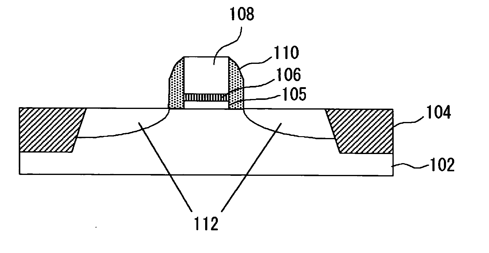
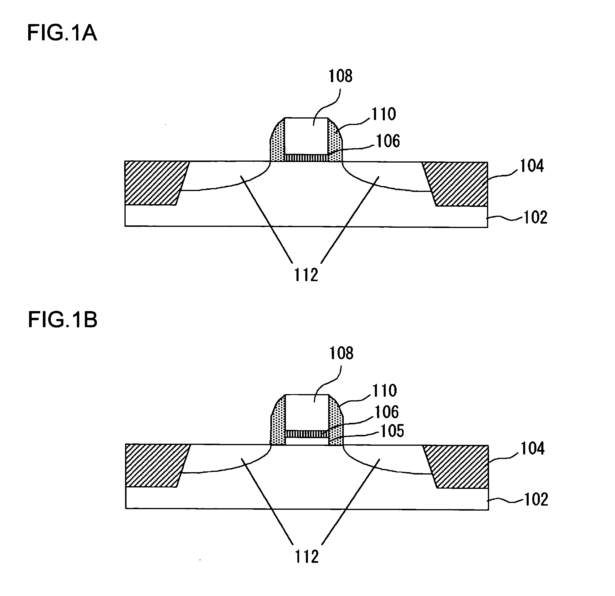
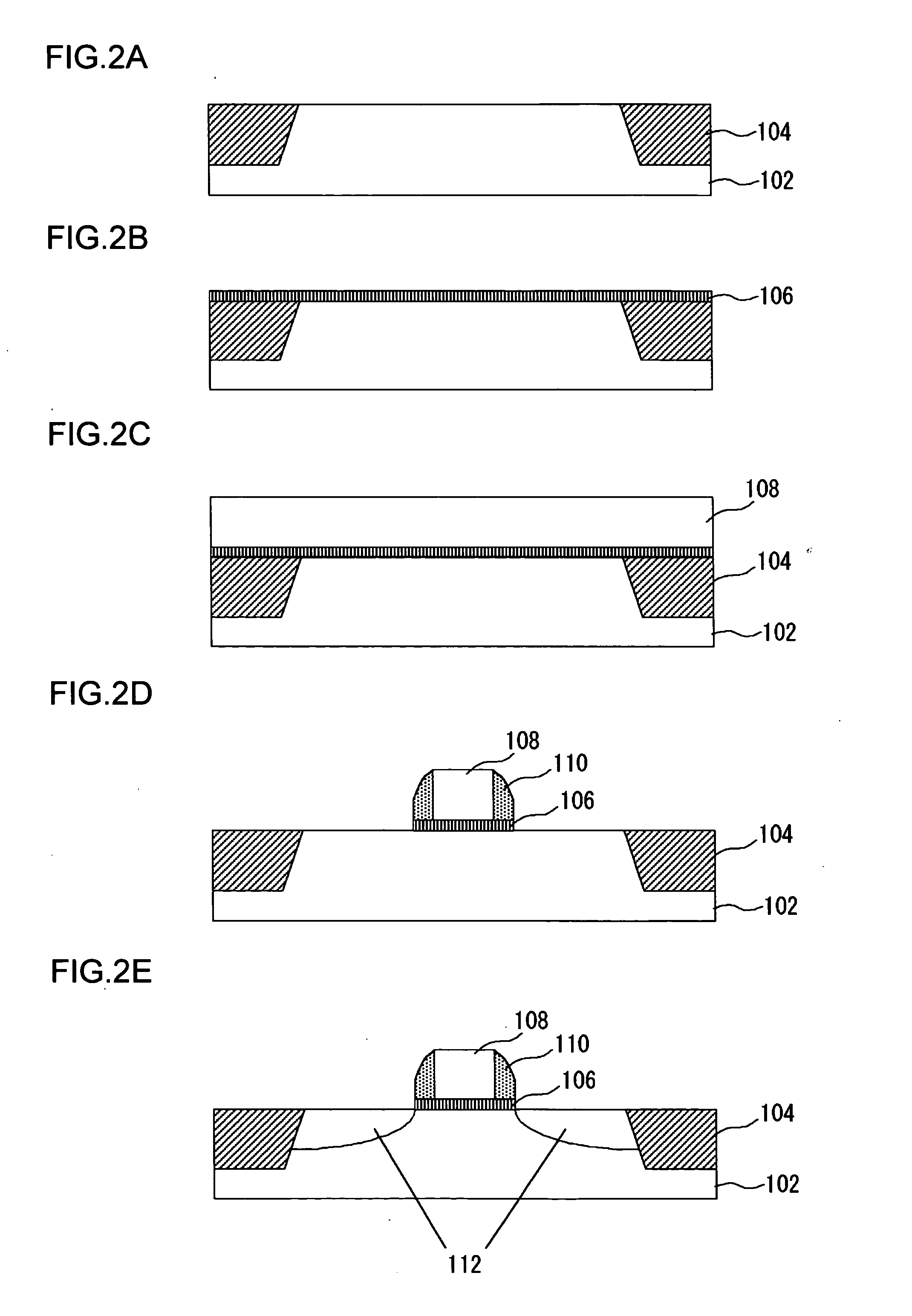
[0045] An MIS transistor of a structure shown in FIG. 1A is fabricated. The process of fabricating the transistor is similar to the one described in the embodiment by referring to FIGS. 2A-2E. The high-K gate dielectric material 106 is produced according to a procedure described by referring to FIG. 3. The high-K gate dielectric material 106 is deposited by the widely practiced ALD method using the film deposition apparatus 200 shown in FIG. 4.

[0046] In this example, a HfAlON film was deposited as the high-K gate dielectric material 106. First, the silicon substrate 102 was cleaned by diluted hydrofluoric acid (DHF) and introduced into the load lock chamber 214 of the film deposition apparatus 200. Subsequently, the silicon substrate 102 was transported to the annealing chamber 212. The silicon substrate 102 was annealed for about 30 seconds in an oxygen atmosphere at about 850-950° C. so as to form a silicon oxide film (interface layer) on the silicon substrate 102. Consequently, ...

first example

[0050] A transistor was fabricated in a process similar to the process of the fifth example except that the ammonia annealing temperature is 650° C. and the oxygen annealing temperature is 650° C.

second example

[0051] A transistor was fabricated in a process similar to the process of the fifth example except that the ammonia annealing temperature is 750° C. and the oxygen annealing temperature is 650° C.


PUM

PropertyMeasurementUnit
temperatureaaaaaaaaaa
binding energyaaaaaaaaaa
temperatureaaaaaaaaaa

Abstract

After the surface of the substrate is cleaned, an interface layer or an antidiffusion film is formed. A metal oxide film is built upon the antidiffusion film Annealing is done in an NH3 atmosphere so as to diffuse nitrogen in the metal oxide film. Building of the metal oxide film and diffusion of nitrogen are repeated several times, whereupon annealing is done in an O2 atmosphere. By annealing the film in an O2 atmosphere at a temperature higher than 650° C., the leak current in the metal oxide film is controlled.

Description

BACKGROUND OF THE INVENTION [0001] 1. Field of the Invention [0002] The present invention relates to a method of fabricating a metallic compound thin film and a semiconductor device including the metallic compound thin film and a method of fabricating the same. [0003] 2. Description of the Related Art [0004] Conventionally, a silicon oxide film, characterized by excellent leak current characteristics and low interface state density, has been used as a gate insulator of a MOSFET. There is a problem, however, that, as the thickness of the gate insulator is decreased in a transistor having a gate insulator formed of a silicon oxide film, as a result of reduction in device size, the gate leak current resulting from a tunnel current is increased. As the gate leak current is increased, a substantial leak current is produced at turn-off, resulting in an abnormal operation of the semiconductor device or an increase in power consumption. Some study has been made in recent years of using a hi...

Claims


Application Information

Patent Timeline
Patent Type & Authority Applications(United States)
IPC IPC(8): H01L21/318H01L21/28H01L21/336H01L21/469H01L29/51H01L29/76H01L29/78H01L31/062H01L31/119
CPCH01L21/28185H01L21/28194H01L29/513H01L29/517H01L29/66575H01L2924/0002H01L29/78H01L2924/00
Inventor IWAMOTO, KUNIHIKOTOMINAGA, KOJINABATAME, TOSHIHIDENISHIMURA, TOMOAKI
Owner ROHM CO LTD
Why Eureka
Try Eureka