Field effect transistor with enhanced insulator structure

a field effect transistor and enhanced insulator technology, applied in the field of field effect transistors, can solve the problems of nominally off hfet devices, and achieve the effect of reducing or eliminating strain generated fields and high density 2deg

Active Publication Date: 2005-06-09
INFINEON TECH AMERICAS CORP
View PDF13 Cites 18 Cited by
  • Summary
  • Abstract
  • Description
  • Claims
  • Application Information

AI Technical Summary

Benefits of technology

[0011] In accordance with the present invention, there is provided a class of devices and methods for operating particular devices that reduce or eliminate strain generated fields and incorporate spontaneous polarization fields in the III-nitride material system. The device is composed of layers of gallium nitride material, such as InAlGaN grown on GaN, such that the in-plane lattice constant of the InAlGaN is substantially for the same as devices, or is much larger than, for nominally off devices, that of GaN. This technique takes advantage of a relatively unused characteristic of gallium nitride material involving spontaneous polarization fields, where previous devices focus on the development of piezoelectric polarization fields to obtain a high density 2DEG.

Problems solved by technology

This results in nominally off HFET devices.

Method used


Image

  • Field effect transistor with enhanced insulator structure
  • Field effect transistor with enhanced insulator structure
  • Field effect transistor with enhanced insulator structure

Examples


Embodiment Construction

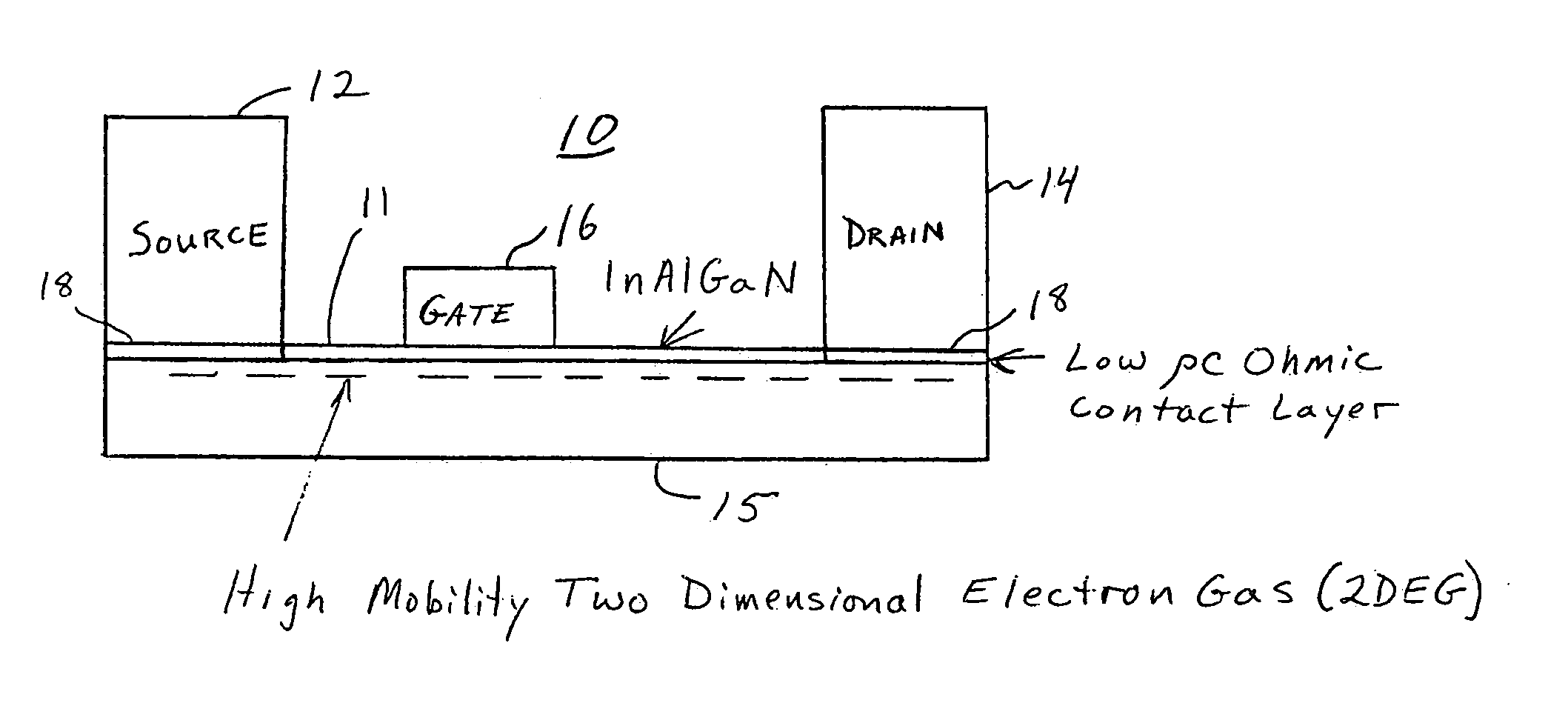
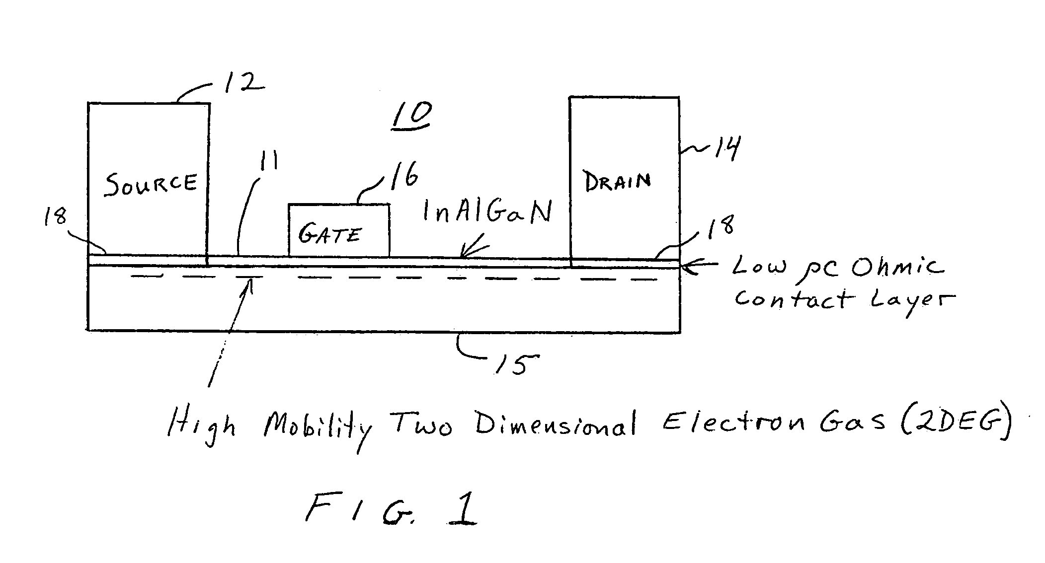
[0023] In the construction of GaN material devices, a number of factors impact the functionality and capability of the devices. A large lattice mismatch between GaN, AlN and InN and the strong piezoelectric and polarization effects in these materials significantly impact the electrical properties of III-nitride heterojunction devices. Nearly all reported GaN-based HEMTs to date use strained GaN-AlGaN junctions with alloy compositions that are designed to maximize the strain in the AlGaN layer, while simultaneously trying to avoid dislocations that may be responsible for long term instabilities in the devices. Various devices and systems for building heterojunction devices have been proposed to control the lattice mismatch and the strain of the GaN-AlGaN junctions. These devices are particularly designed to take advantage of piezoelectric and spontaneous polarization effects and to minimize long term instabilities.

[0024] HFETs typically have three terminals including a gate, a drain...


PUM


Abstract

A III-nitride based field effect transistor obtains improved performance characteristics through manipulation of the relationship between the in-plane lattice constant of the interface of material layers. A high mobility two dimensional electron gas generated at the interface of the III-nitride materials permits high current conduction with low ON resistance, and is controllable through the manipulation of spontaneous polarization fields obtained according to the characteristics of the III-nitride material. The field effect transistor produced can be made to be a nominally on device where the in-plane lattice constants of the material forming the interface match. A nominally off device may be produced where one of the material layers has an in-plane lattice constant that is larger than that of the other layer material. The layer materials are preferably InAlGaN/GaN layers that are particularly tailored to the characteristics of the present invention.

Description

CROSS-REFERENCE TO RELATED APPLICATION [0001] The present application is based on and claims benefit of U.S. Provisional Application No. 60 / 527,631 filed Dec. 5, 2003, entitled InAlGaN FET With Enhanced Insulator Structure, to which a claim of priority is hereby made.BACKGROUND OF THE INVENTION [0002] 1. Field of the Invention [0003] The present invention relates generally to a class of field effect transistors based on III-nitride materials, and relates more particularly to a field effect transistor that uses spontaneous polarization fields to provide enhanced conductivity while providing improved electrical insulation under the gate structure. [0004] 2. Description of Related Art [0005] Development of devices based on III-nitride materials has generally been aimed at high power-high frequency applications such as emitters for cell phone base stations. The devices fabricated for these types of applications are based on general device structures that exhibit high electron mobility a...

Claims


Application Information

Patent Timeline
Patent Type & Authority Applications(United States)
IPC IPC(8): H01L29/20H01L29/778
CPCH01L29/7787H01L29/2003
Inventor BEACH, ROBERT
Owner INFINEON TECH AMERICAS CORP
Why Eureka
Try Eureka